Memory & Libraries IP for TSMC
Welcome to the ultimate
Memory & Libraries IP
for
TSMC
hub! Explore our vast directory of
Memory & Libraries IP
for
TSMC
All offers in
Memory & Libraries IP
for
TSMC
Filter
Compare
746
Memory & Libraries IP
for
TSMC
from
30
vendors
(1
-
10)
-
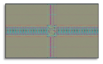
High Speed Single Port Compiler on TSMC 40nm ULP
- Low voltage
- Ultra low power data retention
- Self biasing
- Soft error immunity
-
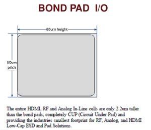
HDMI, LVDS, RF and Analog Pads in TSMC 45/40nm
- A 1.0V to 5V Analog I/O library that includes an HDMI, LVDS, and Analog/RF Low Capacitance pad set in TSMC 45/40nm HPM process.
- This library is collection of analog only IO and Power/Ground pads that include ESD. The target applications are high performance analog interfaces including HDMI, RF, LVDS, basic analog and other applications.
- The pads include a host of specialty features including fail safe, low capacitance, high ESD protection, and IEC robustness.
-
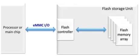
TSMC 22ULL 1.8V/3.3V SD/eMMC PHY AG2
- Synopsys SD/eMMC PHY provides an optimal balance for cost and performance for storage solutions
- Synopsys SD/eMMC PHY is a hard IP that can be used to implement a single interface that can accomplish 4-bit, 8-bit eMMC & 4-bit SD operations
- It includes an optional digi logic circuitry which is required for high-speed operations
- It complies with eMMC 5.1 (JESD84-B51A) and SDIO 6.0 JEDEC standards

-
TSMC N3E SD/eMMC PHY North/South Poly Orientation
- Synopsys SD/eMMC PHY provides an optimal balance for cost and performance for storage solutions
- Synopsys SD/eMMC PHY is a hard IP that can be used to implement a single interface that can accomplish 4-bit, 8-bit eMMC & 4-bit SD operations
- It includes an optional digi logic circuitry which is required for high-speed operations
- It complies with eMMC 5.1 (JESD84-B51A) and SDIO 6.0 JEDEC standards

-
TSMC N3P SD/eMMC PHY North/South Poly Orientation
- Synopsys SD/eMMC PHY provides an optimal balance for cost and performance for storage solutions
- Synopsys SD/eMMC PHY is a hard IP that can be used to implement a single interface that can accomplish 4-bit, 8-bit eMMC & 4-bit SD operations
- It includes an optional digi logic circuitry which is required for high-speed operations
- It complies with eMMC 5.1 (JESD84-B51A) and SDIO 6.0 JEDEC standards

-
TSMC N5 SD/eMMC PHY North/South Poly Orientation
- Synopsys SD/eMMC PHY provides an optimal balance for cost and performance for storage solutions
- Synopsys SD/eMMC PHY is a hard IP that can be used to implement a single interface that can accomplish 4-bit, 8-bit eMMC & 4-bit SD operations
- It includes an optional digi logic circuitry which is required for high-speed operations
- It complies with eMMC 5.1 (JESD84-B51A) and SDIO 6.0 JEDEC standards

-
TSMC N4P SD/eMMC PHY North/South Poly Orientation
- Synopsys SD/eMMC PHY provides an optimal balance for cost and performance for storage solutions
- Synopsys SD/eMMC PHY is a hard IP that can be used to implement a single interface that can accomplish 4-bit, 8-bit eMMC & 4-bit SD operations
- It includes an optional digi logic circuitry which is required for high-speed operations
- It complies with eMMC 5.1 (JESD84-B51A) and SDIO 6.0 JEDEC standards
-
M31 eMMC/SDIO at TSMC 22ULL Process
- Supports HS400 (400Mbps), HS200 (200Mbps), High-speed DDR (52Mbps) and etc.
- Consisting of driver, receiver & pull-up/down resistors
- Power-sequence free
- Provides multi-driving-strength selection
-
M31 eMMC/SDIO at TSMC 22ULP Process
- Supports HS400 (400Mbps), HS200 (200Mbps), High-speed DDR (52Mbps) and etc.
- Consisting of driver, receiver & pull-up/down resistors
- Power-sequence free
- Provides multi-driving-strength selection

-
