Memory & Libraries IP for Samsung
Welcome to the ultimate
Memory & Libraries IP
for
Samsung
hub! Explore our vast directory of
Memory & Libraries IP
for
Samsung
All offers in
Memory & Libraries IP
for
Samsung
Filter
Compare
13
Memory & Libraries IP
for
Samsung
from
7
vendors
(1
-
10)
-
Samsung 8LPU 3.3V SD/eMMC PHY
- Synopsys SD/eMMC PHY provides an optimal balance for cost and performance for storage solutions
- Synopsys SD/eMMC PHY is a hard IP that can be used to implement a single interface that can accomplish 4-bit, 8-bit eMMC & 4-bit SD operations
- It includes an optional digi logic circuitry which is required for high-speed operations
- It complies with eMMC 5.1 (JESD84-B51A) and SDIO 6.0 JEDEC standards
-
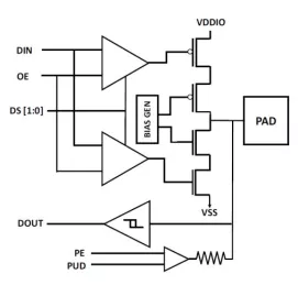
1.8V/3.3V Switchable GPIO with 5V I2C Open Drain and Analog Cells in Samsung 11nm
- A Samsung 11nm Flip-Chip I/O library with dynamically switchable 1.8V/3.3V GPIO with fail-safe capability, 5V I2C / SMBus open-drain cell, 5V OTP cell, 1.8V 3.3V analog cells, and associated ESD.
- A key attribute of this library is its ability to detect and dynamically adjust to a VDDIO supply of 1.8V or 3.3V during system operation.
- The GPIO cell can be configured as input, output, open source, or open drain with an optional internal 50K ohm pull up or pull down resistor.
-
Samsung 5LPE 1.8V/3.3V SD/eMMC PHY AP2
- Synopsys SD/eMMC PHY provides an optimal balance for cost and performance for storage solutions
- Synopsys SD/eMMC PHY is a hard IP that can be used to implement a single interface that can accomplish 4-bit, 8-bit eMMC & 4-bit SD operations
- It includes an optional digi logic circuitry which is required for high-speed operations
- It complies with eMMC 5.1 (JESD84-B51A) and SDIO 6.0 JEDEC standards
-
Samsung 8LPU 1.8V/3.3V SD/eMMC PHY AP1
- Synopsys SD/eMMC PHY provides an optimal balance for cost and performance for storage solutions
- Synopsys SD/eMMC PHY is a hard IP that can be used to implement a single interface that can accomplish 4-bit, 8-bit eMMC & 4-bit SD operations
- It includes an optional digi logic circuitry which is required for high-speed operations
- It complies with eMMC 5.1 (JESD84-B51A) and SDIO 6.0 JEDEC standards
-
Samsung 28nm FDSOI 1.8v/1.0v LVDS Transmitter
- Process: Samsung 28nm FDSOI process
- Supply voltage: 2.25V<=VDD25<=2.75V, 0.9V<=VDD10<=1.1V 1.62V<=VDD18<=1.98v
- Mos device: pfet, nfet, egpfet, egnfet, rpposab
- Operating current:VDD25<24mA
-
LVDS Driver/Buffer
- Available as LVDS driver and buffer configurations
- SLVS solutions
- Combo LVDS + GPIO solutions
- Available in Samsung 28FDS, 14LPP, 11LPP, 10LPP, 8LPP, 5LPP, 4LPPn
-
Embedded OTP (One-Time Programmable) IP, 4Kx32 bits for 0.9V/1.8V FDS
- Logic Embedded IP
- Programming NeoFuse cell by using quantum tunneling mechanism
- High yield performance
- Small IP size