From "What-If" to "What-Is": Cadence IP Validation for Silicon Platform Success
Data rates are escalating with seemingly no end in sight due to the insatiable demand for more bandwidth to accommodate AI factories and other data-intensive AI/ML, HPC, cloud, and data center applications. As just one example, the new PCI Express (PCIe) 7.0 specification doubles the bandwidth over its predecessor—boasting a raw bit rate of 128.0 GT/s for a maximum bandwidth of 512 GB/s bidirectionally in a 16-lane configuration. Ensuring that PCIe, Universal Chiplet Interconnect Express (UCIe), advanced memory subsystems, and other blazing high-speed protocols are electrically sound and will function as intended in the system for which they are designed is no small feat.
Bringing up a new system on chip (SoC) often means diving into firmware bring-up, configuring registers, and validating multi-lane links—tasks that can easily stretch your debug calendar for weeks.
But what if you could streamline that process?
Imagine shortening the bring-up cycle from weeks to days, working with IP that’s already verified in silicon, and eliminating uncertainty from day one—even in complex multi-lane scenarios.
At Cadence, we transform “what-if” into “what-is” with our extensive IP validation expertise, gained through more than 5 years providing full-subsystem testchips for the industry’s leading protocols. Integrating both a PHY and a controller on a single die, Cadence IP subsystems support PCIe, Ethernet, memory, and UCIe protocols (see Figure 1). These integrated, scalable solutions let you validate under true system conditions, uncover corner-case failures early, and shrink your debug schedule from weeks to days.
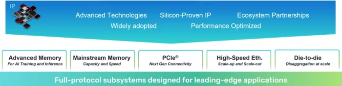
Figure 1: Cadence Interface IP Key HPC/AI Portfolio
Taking validation to the next level, Cadence’s complete PHY and controller subsystem architecture delivers three clear advantages. Our customers can be assured of:
- A real-system multi-lane validation environment rather than an FPGA emulation workaround
- Simpler, more stable hardware setups without auxiliary FPGA boards
- The elimination of FPGA timing-closure headaches and costly FPGA platforms to accommodate controller RTL
These subsystem strengths form the backbone of our flow. With real-world traffic streaming through these multi-lane slices of silicon, corner-case issues surface early, and debug schedules shrink dramatically.
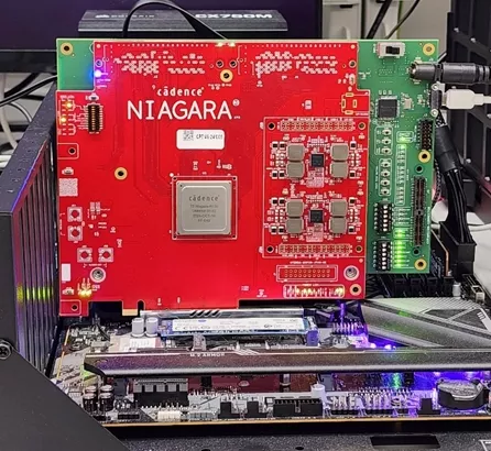
Figure 2: Cadence IP for PCIe 6.0 Full Subsystem Demo
To further ensure you catch every issue before it slows you down, the Cadence validation engine never sleeps. With state-of-the-art test equipment and infrastructure across our labs in India, North America, and Ireland, we are fully equipped to host customer silicon for development, bring-up, and debugging activities around the clock. This global infrastructure has fueled industry-first achievements—including DDR5 12.8Gbps MRDIMM, LPDDR6, and 32Gbps UCIe-S silicon validation—while also supporting key milestones such as PCIe 5.0 x8 and 100G Ethernet IEEE802.ck compliance. In addition, it powers comprehensive test suites:
- Protocol-compliance / interoperability regression
- Electrical characterization (such as functionality testing, receiver jitter tolerance, and transmitter testing)
- Exhaustive reliability and stress testing (such as electrostatic discharge, latch-up, and high-temperature operating life)
Our experts rotate through time zones, share unified dashboards for real-time insights, and pivot instantly to address customer-specific scenarios. This ensures any issues surface early and get resolved without delay.
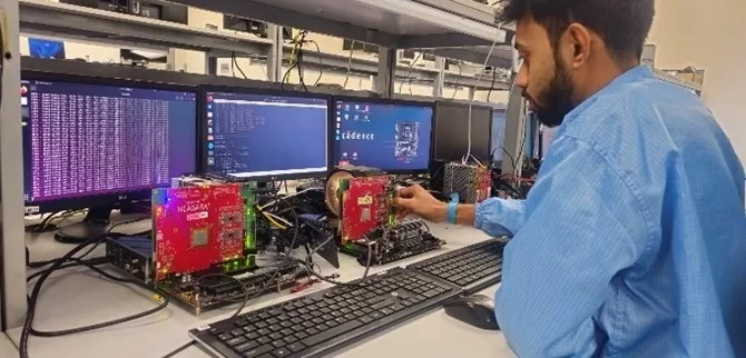
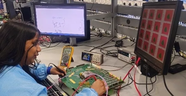
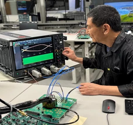
Figure 3: Cadence Professional Lab Environments and Validation Capabilities
By leveraging unified multi-lane subsystem testchips and 24/7 global lab support, Cadence delivers a streamlined validation platform that slashes bring-up cycles, eliminates first-pass uncertainty, and accelerates time-to-market—empowering teams to ship interfaces that work flawlessly from day one.
Ready to leave first-silicon uncertainty behind? Head to cadence.com to unleash your imagination and build next-gen products with speed, precision, and confidence.
Related Semiconductor IP
- SHA-256 Secure Hash Algorithm IP Core
- EdDSA Curve25519 signature generation engine
- DeWarp IP
- 6-bit, 12 GSPS Flash ADC - GlobalFoundries 22nm
- LunaNet AFS LDPC Encoder and Decoder IP Core
Related Blogs
- Cadence Silicon Success of UCIe IP on Samsung Foundry’s 5nm Automotive Process
- The Road to Innovation with Synopsys 224G PHY IP From Silicon to Scale: Synopsys 224G PHY Enables Next Gen Scaling Networks
- Cadence Adds 10 New VIP to Strengthen Verification IP Portfolio for AI Designs
- Rambus CXL IP: A Journey from Spec to Compliance
Latest Blogs
- Area, Pipelining, Integration: A Comparison of SHA-2 and SHA-3 for embedded Systems.
- Why Your Next Smartphone Needs Micro-Cooling
- Teaching AI Agents to Speak Hardware
- SOCAMM: Modernizing Data Center Memory with LPDDR6/5X
- Bridging the Gap: Why eFPGA Integration is a Managed Reality, Not a Schedule Risk