Special IP
Welcome to the ultimate Special IP hub! Explore our vast directory of Special IP
All offers in
Special IP
Filter
Compare
321
Special IP
from
11
vendors
(1
-
10)
-
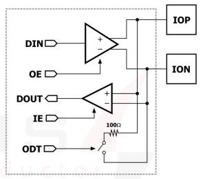
0.9V SLVS Transceiver in TSMC 22nm
- This SLVS I/O Library, implemented in TSMC 22nm with an 11P7M_5X1Z UT-AlRDL metal stack, provides a 0.9V differential transceiver optimized for low-power, high-speed operation.
- Supporting data rates up to 200 Mbps and compliant with JESD8-13 SLVS standards, the library features strong power supply rejection, integrated 100 on-die termination, and robust 2 kV HBM / 500 V CDM ESD protection.
-
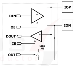
1.2V SLVS Transceiver in UMC 110nm
- This library delivers a compact and reliable 1.2V SLVS transceiver solution in UMC 110nm, optimized for high-speed, low-power applications.
- Featuring robust supply and ground noise rejection, 2kV HBM ESD protection, and integrated on die termination, this library provides both transmit and receive paths compliant with JESD8-13 SLVS standards at up to 200 Mbps.
-
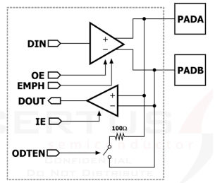
SLVS Transceiver in TSMC 28nm
- This 1.8V SLVS transceiver is a high-performance, low-power I/O solution optimized for TSMCs 28nm process.
- Designed with 1.8V thick oxide devices and a standard low-voltage core interface at 0.8V, this transceiver ensures robust operation across a wide temperature range (-40°C to 125°C).
- Supporting high-speed differential signaling up to 2Gbps, it delivers ex- ceptional signal integrity with low jitter and precise eye diagrams.
-
Wirebond Digital and Analog Library in TSMC 65nm
- A mixed Digital and Analog Library, compatible with I2C and I3C Protocols.
- This library is a mixed Digital and Analog library built for the TSMC 65nm process.
- It is based around a Fail-Safe General Purpose Input/Output (FSGPIO) cell that is compatible with both I2C and I3C protocols.
-
5V ESD Clamp in GlobalFoundries 180nm LPe
- A GlobalFoundries 180nm LPe Specialized 5V ESD Clamp.
- A key attribute of this 5V Clamp is that it can be used for either signal protection or 1.8V power supplies.
- The clamp is a single cell, 44um x 32um in size. It is built from the substrate to metal 6.
-
Wirebond I/O Library in TSMC 130nm
- A radiation-hardened TSMC 130nm Wirebond I/O Library with 3.3V GPIO, 3.3V LVDS TX & RX, 3.3V I2C ODIO, 3.3V Analog cell, OTP cell, and associated ESD.
- Key attributes of this silicon-proven, radiation hardened I/O library include an extended operational temperature range (-50C to 200C), a sleep retention mode, and a built in power regulation PMOS device for core VDD.
-
I/O Library in TSMC 130nm 5V Gen3 BCD
- A TSMC 130nm Wirebond/Flipchip compatible I/O Library with 5V GPIO, 5V ODIO, 5V Analog I/O and 5V Power Supply I/O.
- This silicon-proven, I/O Library features a 5V General Purpose I/O, 5V Open-Drain I/O, 5V Analog I/O, 5V Power Supply and an area efficient 5V ESD protection scheme.
-
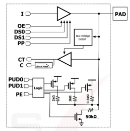
Ultra-low leakage I/O Library in TSMC 22nm
- A TSMC 22nm Wirebond / Flipchip I/O library with dynamically switchabe 1.8V/3.3V GPIO, 3.3V I2C ODIO, 3.3V Analog Cell and associated ESD.
- This is an ultra-low leakage library. The GPIO has a worst-case leakage of only 425nA.
- It works with a wide VDDIO supply range from 1.8V to 3.3V during system operation without the need for the customer to manually switch between high and low-voltage modes.
-
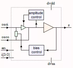
5MHz-35MHz Low Power Crystal Oscillator - TSMC 0.18µ
- 4MHz-35MHz Frequency range.
- No external bias or limit resistors required.
- Current optimization for best power at frequency.
- Amplitude control loop.
- The OSCI pad input can be used as a CMOS input for test.
- Uses single 1.8V supply.
- Enable/power down provision.
-
I3C IO
- 3.3 Volt bi-directional IO capability and multi-voltage capability (1.8V to 3.3V).
- This combo IO supports MIPI I3C IO specifications in 1.8V to 3.3V range.
- Supports I2C SM/FM/FM+ specifications in 1.8V to 3.3V range.