DDR5 IP
Welcome to the ultimate DDR5 IP hub! Explore our vast directory of DDR5 IP
All offers in
DDR5 IP
Filter
Compare
406
DDR5 IP
from
25
vendors
(1
-
10)
-
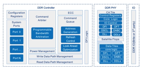
High Speed DDR Interface Solution
- Brite provides a complete DDR subsystem including not only controller, PHY and IO, but also corresponding tuning and configuration software. And this solution can support LPDDR2, DDR3, LPDDR3, DDR4 and LPDDR4/4x combo PHY with the data rate from 667Mbps to 4266Mbps.
-
DDR5 LRRDIMM Verification IP
- Compliant to JEDEC DDR5 SDRAM Specification, Data Buffer & RCD Specification.
- Supports connection to any DDR5 Memory Controller IP communicating with a JEDEC compliant DDR5 Memory Model.
- Supports configurable SDRAM addressing of different sizes (x4, x8 and x16).
- Available in all memory sizes up to 64 Gb.
- Supports for all speed-grades/speed-bins.
-
DDR5 RDIMM Verification IP
- The DDR5 RDIMM Verification IP provides an effective & efficient way to verify the components interfacing with DDR5 RDIMM interface of an ASIC/FPGA or SoC.
- The DDR5 RDIMM VIP is fully compliant with Standard DDR5 specification from JEDEC.
- This VIP is a light weight with an easy plug-and-play interface so that there is no hit on the design time and the simulation time.

-
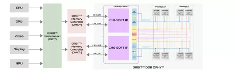
DDR5 MRDIMM PHY and Controller
- The DDR5 12.8Gbps MRDIMM Gen2 PHY and controller memory IP system solutions double the performance of DDR5 DRAM.
- The DDDR5 12.8Gbps design and architecture address the need for greater memory bandwidth to accommodate unprecedented AI processing demands in enterprise and data center applications, including AI in the cloud.
-
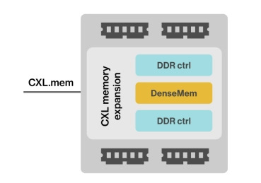
CXL memory expansion
- Turn key solution: compression, compaction, memory management
- Automatic compressed memory tier
- Multi-instance support to match interface throughput
- Cache line granularity decompression for highest read performance (proprietary algorithm)
-
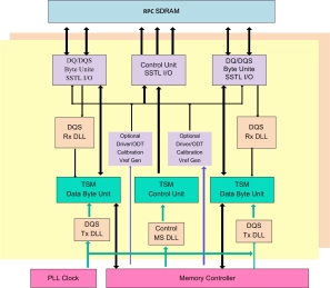
PSRAM/RPC PHY & Controller
- The DDR IP Mixed-Signal MR PSRAM PHY and RPC PHY provide turnkey physical interface solutions for ICs requiring access to JEDEC compatible PSRAM/RPC devices
- It is optimized for low-power and high-speed applications with robust timing and small silicon area
- The PSRAM PHY supports AP memory UHS/OPI PSRAM components on the market, and the RPC PHY supports ETRON components on the market
-
MRDIMM DDR5 & DDR5/4 PHY & Controller
- The DDR IP Mixed-Signal MRDIMM DDR5 PHY and DDR5/4 Combo PHY provide turnkey physical interface solutions for ICs requiring access to JEDEC compatible SDRAM or MRDIMM/ RDIMM/ LRDIMM/ UDIMM DDR5 devices
- It is optimized for low-power and high-speed applications with robust timing and small silicon area
- It supports all JEDEC DDR5/4 SDRAM components in the market
-
GDDR6X/6 Combo PHY & Controller
- The GDDR6X/6 PHY is fully compliant with the JEDEC GDDR6X/6 standard, supporting data rates of up to 20Gbps per pin for PAM2 GDDR6 mode and 24Gbps for PAM4 GDDR6X mode
- The GDDR6X/6 interface supports 2 channels, each with 16 bits for a total data width of 32 bits per memory device
- With a maximum speed of 20/24Gbps per pin, The GDDR6X/6 Combo PHY delivers a peak bandwidth of up to 80GB/s or 96GB/s per memory device
-
GDDR6 PHY IP for 12nm
- JEDEC JESD250 compliant GDDR6 support
- X16 mode, X8 mode, and pseudo-channel mode
- Low frequency RDQS mode support
-
LPDDR5X/5/4X/4 PHY IP for 12nm
- Compliant with JEDEC standards for LPDDR5X/5/4X/4 with PHY standards
- DFI 5.0 Interface Compliant
- Supports up to 4 ranks
- Multiple frequency states
