PCI Express Controller IP
Welcome to the ultimate PCI Express Controller IP hub! Explore our vast directory of PCI Express Controller IP
All offers in
PCI Express Controller IP
Filter
Compare
195
PCI Express Controller IP
from
36
vendors
(1
-
10)
-
Configurable PCI Express 4.0 Link Controller
- Compliant with "PCI Express™ Base Specification, Rev. 4.0 Version 1.0"
- Compliant with "PHY Interface For the PCI Express, SATA, and USB3.1 Architectures"
-
PCIe PHY and controller solution
- Brite 16Gbps PCIe PHY and controller solution provide high efficient interconnection that is optimized for PPA performance. The System can support short-reach or long-reach channels for plenty application scenarios.
- Brite PCIe controller to AXI architecture provides a high-performance, easy-to-use interconnect solution between PCI Express and the latest version of the AXI protocol. It inherits the leading architecture and features an AXI user interface with built-in DMA, compliant with the AMBA® AXI3 and AXI4 specifications.
-
PCIe Controller IP
- The PCI Express® (PCIe®) Controller IP is a highly configurable, performance-optimized core designed for ASIC and FPGA integration.
- Supporting PCIe Gen1 through Gen6 at data rates up to 64 GT/s, the controller accommodates a wide range of link widths (x1–x16) and protocol features to meet the demands of next-generation SoC, networking, and high-performance computing platforms.
- The controller seamlessly interoperates with PIPE-compliant PHYs and supports multiple modes including Root Complex, Endpoint, Switch, and Dual-Mode operation.
-
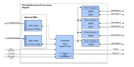
PCIe Multi-Function Option for DMA IP Cores
- The PCI Express specification allows endpoints that incorporate several physical PCIe functions that share the same PCIe connection. Such endpoints are called multi-function devices.
- The big advantage of a multi-function device is, that a separate device driver can be associated to each physical function.
- This simplifies driver development and maintenance significantly by separating the peripheral functions logically into different device drivers.
-
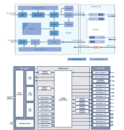
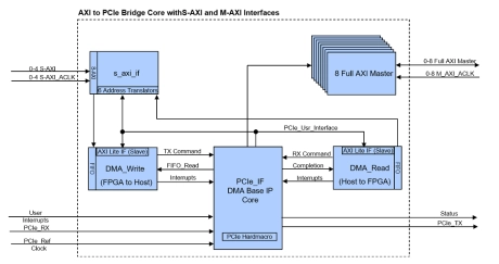
AXI Bridge for PCIe IP Core
- The AXI Bridge for PCIe IP core is the IP solution with a powerful mix of multiple industry standard memory mapped AXI Interfaces.
- The AXI Bridge IP core translates the AXI4 memory read or writes to PCI-Express Transaction Layer Packets and translates PCIe memory read and write requests to AXI4 transactions.
- All interfaces support fully parallel operation without any interferences. Interfaces that are not required can be turned off individually and do not occupy logic resources.
-
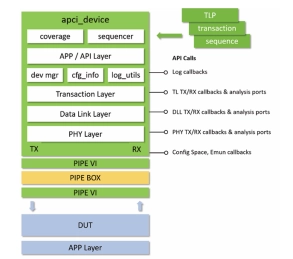
Verification IP for PCIe
- Accelerated confidence in simulation-based verification of RTL designs with PCI Express (PCIe) interfaces: PCIe Gen2/3/4/5/6/7
-
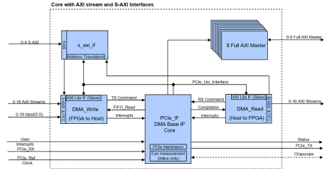
AXI Bridge with DMA for PCIe IP Core
- The AXI Bridge with DMA IP core is the ultimate PCIe DMA IP solution with a powerful mix of multiple industry standard AXI Interfaces.
- AXI Stream interfaces allow continuous data streaming from FPGA to Host or from Host to FPGA. S-AXI Memory mapped interfaces allow easy data access of remote memories in order to realize shared memory access or per to peer applications.
-
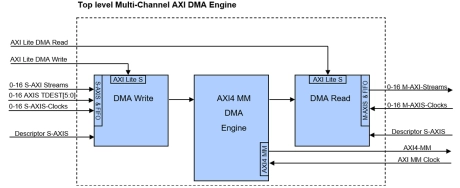
Multi-Channel AXI DMA Engine
- The Multi-Channel AXI DMA engine IP Core for AXI4 is a powerful programmable AXI Stream to AXI memory mapped bridge with sophisticated data addressing options.
- These features allow data accesses on a tile basis in order to address regions of interest (ROI) based applications like stereo cameras, 2D picture compression algorithms and others.
-
PCIe End Point IP Core
- The PCI Express End Point is a high-speed, high-performance, and low-power IP core that is fully compliant to the PCI Express Specification 1.1 and 2.0.
- The IP core is designed for applications in computing, networking, storage, servers, wireless, and consumer electronics.
-
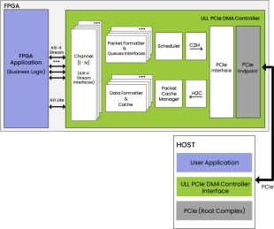
ULL PCIe DMA Controller
- The ULL PCIe DMA Controller is a high-performance, bidirectional data transfer solution. It is designed for seamless communication between FPGAs and host CPUs over PCIe.
- With a round-trip time as low as 585ns*, this IP core empowers developers to maximize resource utilization and achieve ultra-low latency without compromising performance.