PLL IP
Welcome to the ultimate PLL IP hub! Explore our vast directory of PLL IP
Here, you will find a variety of PLL designs and architectures, each tailored to specific application needs, including fractional-N PLLs, integer-N PLLs, and Delay-Locked Loops (DLLs). These variants offer different advantages, such as reduced phase noise, higher frequency stability, and improved design flexibility. Additionally, some advanced PLL IPs incorporate features like spread spectrum clocking to minimize electromagnetic interference, making them suitable for use in sensitive electronic environments.
All offers in
PLL IP
Filter
Compare
1,866
PLL IP
from
55
vendors
(1
-
10)
-
High Speed Integer PLL IP
- Up to 4Ghz clock output
- Wide range of multiplicand
- Small physical area
- TEST pin integrated
-
1.7GHz Multiplying PLL on TSMC 28nm
- Including Loop-filter
- VCO operating range : 850MHz - 1700 MHz
- Output frequency range : 850MHz -1700 MHz
- Input frequency range : 9.6MHz - 216MHz
-
5GHz Multiplying PLL on TSMC 28nm
- Including Loop-filter
- VCO operating range : 2500MHz - 5000 MHz
- Output frequency range : 1250MHz - 2500 MHz
- Input frequency range : 12MHz - 320 MHz
-
1.8GHz SSCG PLL on TSMC 28nm HPC+
- Including Loop-filter
- VCO operating range : 900MHz - 1800 MHz
- Output frequency range : 900MHz-1800 MHz
- Input frequency range : 12MHz - 192MHz
-
3.2GHz SSCG PLL on TSMC 12nm
- Including Loop filter
- VCO operating range : 1600MHz- 3200MHz
- Output frequency range: 400MHz- 3200MHz
- Input frequency range : 10MHz- 200MHz
-
4.3GHz SSCG PLL on TSMC 7nm
- Including Loop filter
- VCO operating range : 2000MHz-4300MHz
- Output frequency range: 500MHz-4300MHz
- Input frequency range : 10MHz- 200MHz
-
Automotive Grade PLLs, Oscillators, SerDes PMAs, LVDS/CML IP
- TSMC IP9000 Alliance member enabling automotive IP support in TSMC automotive processes
- Automotive Documentation including Safety Manual, FMEDA and DFMEA
- Design reliability report containing EM/IR and Aging analysis
-
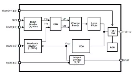
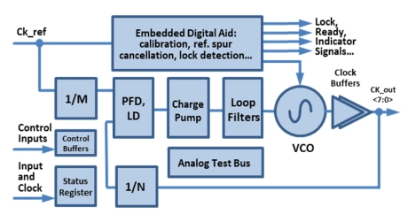
General use, integer-N 4GHz Hybrid Phase Locked Loop on TSMC 28HPC
- This Integer-N Hybrid (Digitally Aided Analog) PLL generates clock signals within broad frequency range.
- Division coefficients of the embedded input and feedback dividers can be set to any integer between 1 and 64 or may be bypassed to save power.
- Higher order dividers and/or pre-scalers are optional.
-
All Digital Fractional-N PLL for Performance Computing in UMC 40LP
- Fractional multiplication with frequency up to 4GHz
- Low jitter (< 10ps RMS)
- Small size (< 0.01 sq mm)
- Low Power (< 5mW)
-
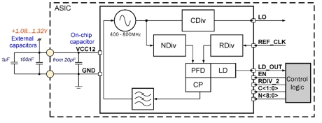
50MHz to 800MHz Integer-N RC Phase-Locked Loop on SMIC 55nm LL
- 055SMIC_PLL_01 forms clock output signal with frequency from 50 to 800MHz.
- It consists of the ring VCO with frequency from 400 to 800MHz, a programmable feedback divider, a low noise digital phase noise detector (PFD), a precision charge pump (CP) with internal loop filter, lock detector (LD) and programmable clock divider to obtain a required output frequency.
- LO output signal is CMOS compatible.