Low Power PLL IP
Welcome to the ultimate Low Power PLL IP hub! Explore our vast directory of Low Power PLL IP
All offers in
Low Power PLL IP
Filter
Compare
13
Low Power PLL IP
from
7
vendors
(1
-
10)
-
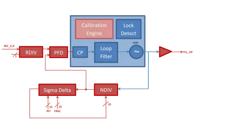
40nm 1.1V 6.0GHz-9.4GHz Fractional-N RF PLL
- TSMC 40nm CMOS
- 6.0GHz-to-9.7GHz Buffered VCO PLL Output Coverage
- Scalable Power Consumption
-
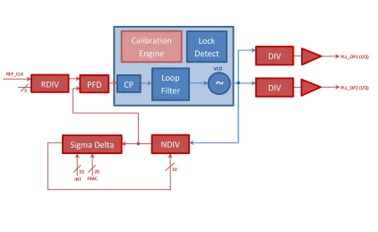
40nm 1.1V 2GHz-4.7GHz Fractional-N RF Quadrature PLL
- 2.0GHz-to-4.7GHz PLL Output Coverage
- Scalable Power Consumption
-
PLL
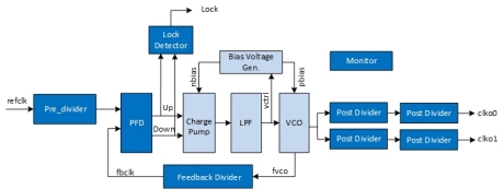
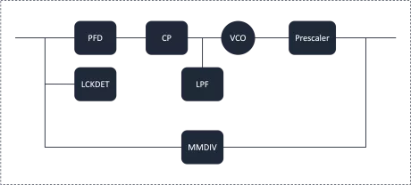
- The high performance PLL is a high speed, low jitter frequency synthesizer, developed as an IP block to reduce time to market, risk, and cost in the development of Analog Front-End design
- It can generate a stable high-speed clock from an ultra-wide input clock
- With excellent supply noise immunity, the PLL is ideal for use in noisy mixed signal SoC environments
-
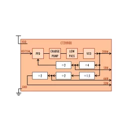
25MHz to 200MHz Low Jitter Low Power PLL
- Fully Differential Topology
- Charge Pump 3rd order configuration
- 2nd order passive loop filter
-
14GHz Integer-N High-Speed PLL
- Type II hybrid Integer-N LC-PLL
- Quadrature clocks at 14GHz and 7GHz
- Fast locking
-
Dual WideBand Frequency Synthesizer with Integrated VCO and Loop Filter
- 3GPP superset LO sub-system (All bands + CA)
- PLL1 [0.49mm2] for LTE with VCO1
- PLL2 [0.76mm2] for LTE&GSM with VCO1 and VCO2
- Small size, high-performance and low-power (24mW)
-
Low jitter 4.96GHz to 5.6GHz PLL in TSMC N40
- Low RJ output – 0.3ps RMS for the primary 5GHz output.
- A built-in bandgap block for the generation of reference voltages/currents.
-
PLL - SMIC 55nm Eflash
- Supports low to 0.9V power supply, the supply range is from 0.90V to 1.32V
- Only one power supply for easy use by customers
- Lower than 70uW power to generate 100MHz output clock with 0.9V power supply
- Supports reference clock from 2MHz to 80MHz
-
PLL - HHGrace 110nm ULL
- Output range: 1MHz~300MHz;
- Operating current: <120uA@100MHz;
- RMS jitter: <15ps;
- Supports 1.20V power supply
-
PLL - HHGrace 110nm ULL
- Generate real time phase aligned clock with short breaks of reference clock;
- Power supply range is from 1.30V to 1.65V
- 1.5V ULL MOS only;
- Lower than 50uA static current;