FD-SOI: A Cyber-Resilient Substrate Against Laser Fault Injection—The Future Platform for Secure Automotive Electronics
By Philippe Flatresse 3, Loïc Mangin 1, Krishna Pradeep 3, Laurent Maingault 1, Rainer Lutz 3, Romain Wacquez 2, Emmanuel Sabonnadière 3
1 Univ. Grenoble Alpes, CEA, LETI MINATEC Campus, F-38054 Grenoble, France
2 CEA-Leti, Centre CMP, Equipe Commune CEA Leti- Mines Saint-Etienne, F - 13541 Gardanne France
3 SOITEC, Automotive Division, F- 38190 Bernin
Abstract
ISO/SAE 21434 elevates hardware security to a first-class requirement in automotive systems, where physical attacks can undermine secure boot, protected debug, and execution integrity. Among physical fault techniques, near-infrared Laser Fault Injection (LFI) is the most precise lab instrument to expose silicon-level vulnerabilities. Fully Depleted Silicon-On-Insulator (FD-SOI) offers intrinsic advantages versus bulk CMOS by suppressing dominant LFI fault mechanisms—diffusion/collection photocurrent and laser-induced IR-drop—through the buried oxide (BOX) isolation. Comparative experiments on 22FDX versus 28 nm bulk show a substantial increase in attack effort and time;in both unprotected AES cryptoprocessor and protected elliptic-curve accelerators, FD-SOI proved up to 150× more resistant. These physical benefits translate into higher assurance levels for schemes such as Common Criteria (CC) and SESIP, directly supporting ISO/SAE 21434 compliance.
Index Terms— FD-SOI, Hardware Security, Laser Fault Injection, Body-Bias, ISO/SAE 21434, Automotive Cybersecurity, Substrate Engineering, Transistor Physics.
I. Introduction: Why Hardware Security Now Matters in Automotive
Modern vehicles integrate increasing digitalization, automation, and pervasive connectivity (Wi-Fi, OTA updates, steer-by-wire). Premium platforms may host 70–100 MCUs, multiplying the cyber-attack surface. Regulatory frameworks have emerged accordingly: ISO/SAE 21434 mandates cybersecurity risk management across the product lifecycle. Within TARA analyses, Fault Injection Attacks (FIA) rank high because they can bypass secure boot, unlock protected debug, or alter program flow.
While voltage glitches and EMFI are field-deployable, LFI—tightly focused near-IR pulsed laser—remains the gold-standard laboratory method to systematically map silicon vulnerabilities with sub-micron spatial and nanosecond temporal control. Backside access, increasingly favored as frontside metal stacks thicken and shielding improves, further prioritizes substrate-level robustness.
FD-SOI, with an ultra-thin silicon film electrically isolated from the handle wafer by the BOX, directly addresses this need by removing silicon-substrate conduits that LFI exploits in bulk CMOS. Beyond passive resilience, FD-SOI’s body-biasing gives designers an active knob to harden devices during certification or secure modes, aligning with “security by design” expectations.
II. Physical Foundations: FD-SOI vs. Bulk CMOS
A. Dominant Bulk Fault Mechanisms Neutralized by FD‑SOI
This section summarizes how near‑IR laser fault injection (LFI) perturbs planar bulk CMOS through substrate‑mediated paths and how FD‑SOI suppresses them.
In bulk, four concurrent mechanisms contribute to fault formation: (i) drain/body charge collection, (ii) laser‑induced IR‑drop on the supply network via well–substrate currents, (iii) funneling and charge diffusion through the substrate, and (iv) parasitic bipolar amplification (vertical and lateral). FD‑SOI’s ultra‑thin active film and buried oxide (BOX) isolate the device from the handle wafer and the supply network, thereby eliminating (i)–(iii) and attenuating (iv) to a residual, lateral‑only effect.
1) Drain/Body Charge Collection (Photocurrent at Reverse‑Biased Junctions): In bulk CMOS, laser‑generated electron–hole pairs drift and diffuse toward reverse‑biased PN junctions (e.g., OFF‑state drains). The transient photocurrent scales approximately with the effective collection volume, The collection voltage is given by Vcol ∝ Aj⋅Ldiff, where Aj is the junction area and Ldiff is the substrate diffusion length. Because both Aj and the available volume are larger in bulk, even a moderately defocused beam can inject sufficient charge to upset a storage node. In FD‑SOI, the active silicon film is only a few nanometers thick and has negligible junction area to the substrate; the buried oxide (BOX) beneath the active layer acts as a barrier that suppresses vertical charge transport. Consequently, Vcol collapses by orders of magnitude, the induced photocurrent is strongly reduced, and this path is intrinsically suppressed. Practically, the XY/Z fault window tightens: successful injections require near‑perfect focusing on the transistor’s active region and higher pulse energy.
2) Laser‑Induced IR‑Drop on Supply Rails (Well–Substrate Conduction): In bulk technologies, N‑wells tied to VDD and the surrounding P‑substrate form “low‑impedance” loops for laser‑induced currents. A localized photo‑current flowing from N‑well to P‑substrate produces a transient drop (or ground bounce), which can corrupt logic or timing far from the illuminated spot via the power grid. Standard FD‑SOI practice avoids this failure mode by keeping wells not hard‑tied to the rails; wells are biased through dedicated body‑bias networks instead. As a consequence, a laser shot cannot inject current into VDD /GND and the IR‑drop mechanism is absent by construction. Implementation caveat: Non‑standard FD‑SOI layouts that short N‑well to VDD (e.g., for convenience or legacy cells) re‑introduce the bulk‑like IR‑drop sensitivity and should be avoided in security‑critical domains.
3) Funneling and Substrate Charge Diffusion: In bulk, two models of collection in the volume of the substrate can contribute to collection of charges at a drain. First electron and holes generated by a laser can diffuse before recombining and then reach a sensitive drain and contribute to the unwanted transient current. Also the transient electric field produced by a high‑energy deposition extends the depletion region and creates a funneling effect that channels carriers into nearby junctions, increasing the collection length micrometers away from the effective Drain/Well junction when laser is off. This broadens the sensitive area and can produce multi‑cell upsets. Moreover, aggressive energy can trigger latch‑up through PNPN parasitic paths spanning wells and substrate. In FD‑SOI, the BOX truncates vertical field lines and stops substrate‑through conduction; funneling is therefore prevented, multi‑cell effects are strongly curtailed, and latch‑up is not observed in digital FD‑SOI because no continuous PNPN path exists across the oxide.
4) Parasitic Bipolar Amplification (Residual Mechanism in FD‑SOI): Both vertical and lateral parasitic bipolar transistors can be activated in bulk, where the substrate provides the base/collector path and a large volume for carrier transport. In FD‑SOI, the vertical component is interrupted by the BOX; only a lateral parasitic bipolar remains within the thin film. Its effective gain is reduced by the small active volume, yielding shorter, lower‑amplitude transients. Importantly, reverse body‑bias (RBB) further suppresses this residual path by increasing the effective threshold and steering minority carriers away from the channel, thereby increasing the laser energy required for a fault. This tunability provides a practical hardening knob during secure modes or certification testing.
To summarize, with diffusion‑collection and IR‑drop removed, funneling blocked, and only a reduced lateral bipolar remaining, FD‑SOI shrinks the spatial/axial sensitivity window, raises the energy threshold, and increases time‑to‑fault, directly elevating the attacker’s cost and the attainable assurance level.
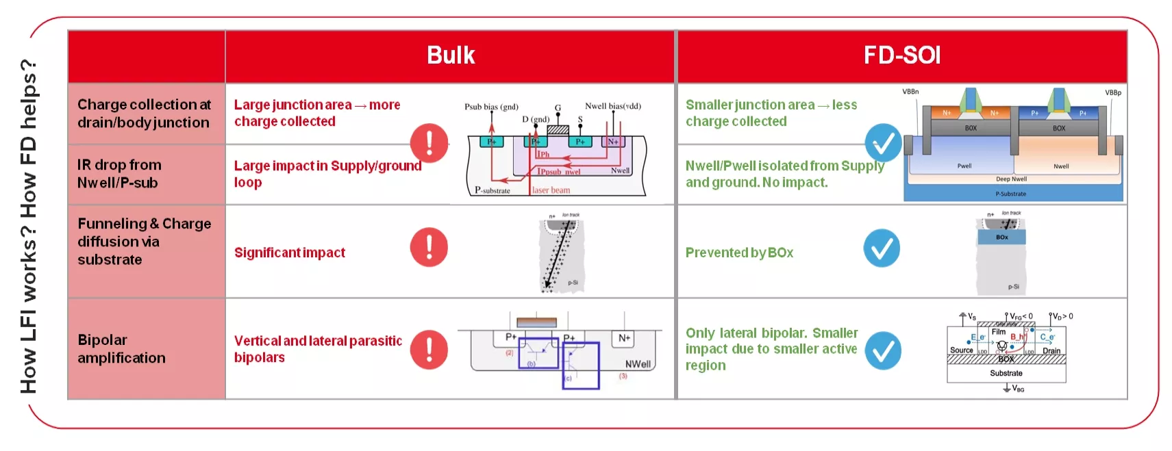
Figure 1. LFI paths in (a) bulk CMOS versus (b) FD-SOI. The BOX in FD-SOI blocks substrate-mediated diffusion and IR-drop spreading.[2,6,7,8,9]
B. The Residual Mechanism in FD-SOI: Parasitic Bipolar Amplification
With diffusion and laser‑induced IR‑drop suppressed by the BOX, LFI‑induced upsets in FD‑SOI are dominated by the activation of a parasitic lateral bipolar transistor confined to the ultra‑thin silicon film (emitter ≈ source, base ≈ body/channel, collector ≈ drain). The BOX breaks any vertical path, so the vertical PNP/NPN present in bulk does not contribute. Two FD‑SOI attributes curb the effectiveness of this residual mechanism:
- Small charge‑collection volume: The few‑nanometer‑thick active film severely limits both the number of photo‑carriers that can be generated and the distance over which they can be transported before recombination. As a result, the effective bipolar gain βeff\beta_\text{eff}βeff and the fault cross‑section shrink relative to bulk because the base region is short, carrier lifetimes are reduced, and no substrate funneling exists. Practically, a tighter XY/Z focus and higher pulse energy are required to sustain the transient collector current needed to upset a node.
- Body‑bias controllability: Applying reverse body‑bias (RBB)—i.e., increasing ∣VSB∣ for NMOS or ∣VBS∣ for PMOS—raises the effective threshold via the body effect ΔVTH≈γ (2ϕF+∣VSB∣−2ϕF), widens the depletion in the body, reduces minority‑carrier injection, and thereby lowers βeff of the lateral parasitic BJT. Empirically, RBB shifts the fault energy threshold upward and narrows the viable Z‑window; forward body‑bias (FBB) has the opposite trend and should be avoided during sensitive operations. This tunability—corroborated by both radiation‑effects literature and FD‑SOI LFI campaigns—provides a practical hardening knob that system software can engage in secure modes without architectural changes.
III. Experimental Evidence: LFI Attack Complexity Increases on FD-SOI
Side-by-side characterizations on 22FDX and 28 nm bulk devices (D-FFs, SRAM bitcells, AES and ECC accelerators) quantify FD-SOI’s advantage.
A. Resistance Metrics and Time-to-Fault
FD-SOI required up to 150× more laser shots than bulk to obtain a usable fault under matched setups. On AES-128 without countermeasures, the time-to-first-fault rose from ≈ 10 min (bulk) to 10 hours (FD-SOI) due to the need for fine spatial scans and higher energy thresholds. Minimum laser power for flips was consistently higher on FD-SOI (e.g., sub-0.3 W flips in bulk vs. ≳ 0.5 W in FD-SOI for comparable test points), consistent with BOX-mediated isolation.
Takeaway: FD-SOI extends attack time, raises energy budget, and narrows viable operating windows, all of which directly increase assurance levels in evaluation schemes.
B. Spatial (XY) and Axial (Z) Sensitivity Windows
- Axial (Z) Focus Window: In bulk, defocused shots can still cause faults; higher power often widens the effective Z window. In FD-SOI, the fault-inducing Z range is narrow (on the order of ± 0.5–1 μm around the optimum focal plane of the active film). Over-powering does not appreciably broaden this window and tends to raise damage risk.
- Lateral (XY) Hotspots: Bulk substrates commonly show micron-scale halos of sensitivity due to lateral diffusion, IR-drop propagation and funnelling. FD-SOI hotspots are sub-micron and sharply localized (e.g., a 200–300 nm area over a specific drain). Zero faults were observed just 0.4–0.5 μm off hotspot centers under conditions that readily faulted bulk. Attackers must therefore scan with ≤ 0.1 μm step sizes, multiplying search time.
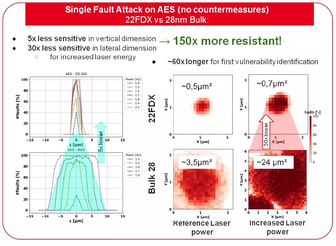
Figure 2. Measured fault probability maps (schematic): (a) bulk exhibits wider XY and Z sensitivity; (b) FD-SOI confines sensitivity to a tight XY hotspot and narrow Z slab.
C. Permanent-Damage Risk as an Attacker Deterrent
On FD-SOI, excess power or aggressive shot counts more frequently led to irreversible failures in memory cells (stuck bits) and sometimes logic, while comparable bulk samples survived. Likely contributors include localized thermal filamentation in the ultra-thin oxide film or BOX charge trapping. Practically, this raises attacker risk: pushing power to “speed up” the search can brick the device and abort the campaign—arguably a fail-safe bias from a defender’s perspective.
IV. Value for Automotive Compliance
A. Mapping Physical Resilience to Assurance Schemes
In ISO/SAE 21434 TARA, the likelihood of successful physical attack decreases when time-to-fault, equipment complexity, and operator expertise increase. FD-SOI elevates all three, improving risk ratings and easing security concept validation.
For CC and SESIP, evaluation families explicitly consider IFA resistance. Empirically longer campaigns (e.g., hours vs. minutes; narrow XY/Z windows; higher power thresholds; damage risk) serve as objective evidence in certification dossiers, helping reach EAL4+-class or higher SESIP levels with fewer additional countermeasures. This shortens certification cycles and reduces BoM/design overhead compared to compensating bulk vulnerabilities in logic alone.
B. Toward a Next‑Generation “Cyber‑Resilient Substrate”
While today’s FD‑SOI already removes the dominant laser–substrate coupling mechanisms, further hardening can be obtained by engineering the wafer itself so that the substrate participates actively in security. Two complementary directions are particularly promising: (i) a buried optical barrier that attenuates and/or reflects near‑IR energy before it reaches the active film, and (ii) substrate‑integrated sensing and identification features that detect, localize, and cryptographically bind the silicon to the product.
A buried optical barrier targets the LFI energy transport path through the handle wafer. The concept is to introduce a thin, highly doped layer (e.g., p+), positioned a few micrometers below the BOX, that exhibits strong free‑carrier absorption at λ≈1064 nm (Drude‑like FCA). By placing this layer in the optical path—yet outside the transistor’s electrostatically active region—the incident backside flux is partially absorbed and scattered before it can generate carriers in the ultra‑thin device film. Beyond attenuation, the barrier can be patterned during substrate processing to embed a wafer‑level watermark—a predetermined, sub‑surface motif that is readable by IR imaging at incoming inspection and acts as a tamper‑proof, anti‑counterfeit feature.
In parallel, substrate‑integrated sensors and PUFs transform the wafer into an always‑on tamper monitor and a root of hardware identity. Distributed perturbation sensors—implemented as shallow photodiodes, bulk‑current pickups, or thermal micro‑sensors placed beneath or around the BOX—can detect fast optical or thermal transients characteristic of LFI. Their outputs feed an always‑on security controller that timestamps events, raises interrupts, or triggers protective responses such as clock gating, entry into a secure RBB mode, or key zeroization, with thresholds tuned to avoid false positives under normal environmental variations. For identity, controlled, sub‑lithographic variations in crystal strain, dopant distribution, or isotopic composition can be introduced at wafer fabrication to realize monocrystalline PUFs whose responses are read electrically (e.g., via body‑bias‑sensitive ring oscillators or threshold monitors). Standard reliability techniques—enrollment, helper data, and fuzzy extractors—stabilize the PUF output across voltage and temperature, enabling repeatable key derivation that binds the SoC to its substrate of origin. Together, these functions elevate the substrate from a passive mechanical support to an active security perimeter that both dissipates the attack energy and signals when an attack is underway.
From an integration standpoint, both approaches are compatible with 300 mm FD‑SOI flows. The optical barrier can be realized by tailored implants or epi layers prior to BOX bonding, with thermal budgets chosen to maintain dopant profiles and BOX integrity. Sensor and PUF structures are co‑designed with the body‑bias network to avoid inadvertent well–rail connections and to preserve FD‑SOI’s immunity to laser‑induced IR‑drop.
These directions align with an end-to-end security stack “from silicon to software”, where substrate features complement transistor- and system-level protections.
V. Conclusion
FD-SOI provides a material-level uplift for hardware security by breaking the substrate pathways that LFI exploits in bulk CMOS. The BOX eliminates diffusion-collection and laser-induced IR-drop, while parasitic bipolar effects can be further controlled via body-bias. Measured outcomes include narrow XY/Z sensitivity windows, higher energy thresholds, longer search times, and a non-trivial damage risk for over-aggressive attackers—collectively yielding up to 150× effective resistance in unprotected crypto blocks.
For automotive programs under ISO/SAE 21434 and UN R155, these advantages reduce residual risk, streamline certification (CC/SESIP), and cut system-level security costs. As substrate engineering advances toward buried optical barriers and integrated anti-tamper/PUF features, FD-SOI is poised to become the reference platform for secure automotive electronics where trust must be anchored at the silicon layer.
This paper is based on research work carried out in the framework of the FAMES Pilot Line of the Chips JU, funded by Horizon Europe grant 101182279 and the ANR NextGen project ANR-22-NEXTG-001 of the France 2030 initiative
References
[1] S. P. Skorobogatov and R. J. Anderson, “Optical Fault Induction Attacks,” in CHES 2002, LNCS 2523, pp. 2–12, 2003. doi: 10.1007/3-540-36400-5_2.
[2] J.-M. Dutertre et al., “Sensitivity to Laser Fault Injection: CMOS FD-SOI vs. CMOS bulk,” in Proc. IEEE IOLTS, pp. 212–217, 2018. doi: 10.1109/IOLTS.2018.8474120.
[3] R. A. C. Viera et al., “Role of Laser-Induced IR Drops in the Occurrence of Faults: Assessment and Simulation,” in Proc. Euromicro DSD, pp. 102–109, 2017. doi: 10.1109/DSD.2017.43.
[4] CEA-Leti and Soitec, “FD-SOI for Enhanced Security – Strategic Partnership Announcement,” Press Release, Grenoble, June 18, 2025.
[5] R. Y. Acharya et al., “Anti-Piracy of Analog and Mixed-Signal Circuits in FD-SOI using Body-Bias Obfuscation,” in Proc. ASP-DAC 2022, pp. 37–42, Jan. 2022. doi: 10.1109/ASP-DAC52403.2022.9712547.
[6] V. Malherbe et al., “Alpha soft error rate of FDSOI 28 nm SRAMs: Experimental testing and simulation analysis”, IEEE IRPS, 2015.
[7] W. Da Cruz et al., “An experimentally tuned compact electrical model for laser fault injection simulation”, IEEE IOLTS, 2022.
[8] Pichon et al., “Theoretical Model of Transient Current in CMOS Inverter Under IR Laser Pulse Responsible of Bitflip in FDSOI Technology”, IEEE TED, 2025.
[9] J.M. Dutertre et al., “Improving the ability of Bulk Built-In Current Sensors to detect Single Event Effects by using triple-well CMOS”, Microelectronics Reliability, 2014.
Related Semiconductor IP
- UALinkSec Security Module
- Quantum Safe, ISO 21434 Automotive-grade Programmable Hardware Security Module
- Embedded Hardware Security Module (Root of Trust) - Automotive Grade ISO 26262 ASIL-B
- Embedded Hardware Security Module for Automotive and Advanced Applications
- Hardware Security Module
Related Articles
- Fault Injection in On-Chip Interconnects: A Comparative Study of Wishbone, AXI-Lite, and AXI
- Interstellar: Fully Partitioned and Efficient Security Monitoring Hardware Near a Processor Core for Protecting Systems against Attacks on Privileged Software
- ShuffleV: A Microarchitectural Defense Strategy against Electromagnetic Side-Channel Attacks in Microprocessors
- SoC Test and Verification -> Leveraging memory for better fault tolerance
Latest Articles
- TensorPool: A 3D-Stacked 8.4TFLOPS/4.3W Many-Core Domain-Specific Processor for AI-Native Radio Access Networks
- Assertain: Automated Security Assertion Generation Using Large Language Models
- VolTune: A Fine-Grained Runtime Voltage Control Architecture for FPGA Systems
- A Lightweight High-Throughput Collective-Capable NoC for Large-Scale ML Accelerators
- Quantifying Uncertainty in FMEDA Safety Metrics: An Error Propagation Approach for Enhanced ASIC Verification