Agile Design for Hardware, Part II
David Patterson and Borivoje NikoliÄ, UC Berkeley
EETimes (7/30/2015 07:00 AM EDT)
In the second of a three-part series, two Berkeley professors suggest its time to apply Agile design techniques to hardware.
We asked readers of Part I to guess the cost of a prototype run of 28 nm chips, as Agile development relies on a sequence of interim prototypes versus the One Big Tapeout of the traditional Waterfall process. Here are the results:
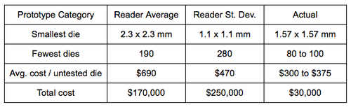
The surprisingly low manufacturing cost of prototype chips—one fifth the readers’ estimate—means Agile development is eminently affordable, even for academics. (See www.AgileSoC.com for more evidence.) It also calls into question the current high cost of designing SoCs using the Waterfall process. Having established Agile’s viability, based on our experience we propose four guidelines to lower development costs.
To read the full article, click here
Related Semiconductor IP
- ReRAM NVM in DB HiTek 130nm BCD
- UFS 5.0 Host Controller IP
- PDM Receiver/PDM-to-PCM Converter
- Voltage and Temperature Sensor with integrated ADC - GlobalFoundries® 22FDX®
- 8MHz / 40MHz Pierce Oscillator - X-FAB XT018-0.18µm
Related Articles
- Agile Design for Hardware, Part I
- How to design secure SoCs, Part II: Key Management
- QiMeng: Fully Automated Hardware and Software Design for Processor Chip
- How to design secure SoCs, Part III: Secure Boot
Latest Articles
- An FPGA-Based SoC Architecture with a RISC-V Controller for Energy-Efficient Temporal-Coding Spiking Neural Networks
- Enabling RISC-V Vector Code Generation in MLIR through Custom xDSL Lowerings
- A Scalable Open-Source QEC System with Sub-Microsecond Decoding-Feedback Latency
- SNAP-V: A RISC-V SoC with Configurable Neuromorphic Acceleration for Small-Scale Spiking Neural Networks
- An FPGA Implementation of Displacement Vector Search for Intra Pattern Copy in JPEG XS