SoC interconnect performance verification methodology based on hardware emulator
Grenoble France
Abstract :
This paper describes an interconnect performance verification methodology which was developed for a complex multi source digital television SoC project. The historical and technical reasons of the interconnect performance verification are detailed in the introduction. Then the verification platform, the hardware measurement agent (called spy), the methodology flow and the measurement method are described. The emulator resource optimization is discussed. This methodology was extended for CPU real time constraints verification.
Introduction:
The explosive growth in the electronic industry over the last 20 years has been enabled by the rapid progress of semiconductor technology which can support now more than 100 million gates per integrated circuit (IC). The complexity moved from numerous circuits soldered on a printed circuit board to a single system on chip (SoC) integrating more and more complex functions. As the circuit complexity was increasing a new methodology was needed in order to split the problem into simpler ones. This methodology is based on reused IP communicating altogether. Each autonomous circuit function was implemented into one hardware block called IP: one function per IP. IP communication was standardised in a hardware interface and a communication protocol. The hardware interface defines all interface signal names and characteristics (electrical and timing). The protocol defines all the data transfer procedures (signal sequences). Communication protocol defines different level of abstraction: messages, packets and transaction cells. Several hardware interfaces and protocol were defined in the industry: VSIA, STbus, OCP, ARM AXI, ARM AHB ….
This IP reused methodology improved the time to market and gained productivity during the design phase. But this methodology transformed one problem into another one. It simplifies the problem of “adding altogether dedicated function to build a system” but created the problem of “IP interaction with the interconnect”: one IP should not fail due to the other simultaneous IP data transfer. This new issue was solved by defining a set of running requirement called “IP system constraints” which defines the minimum set of rules that a system should meet in order to guaranty that an IP works as specified once integrated in a SoC. If one of these constraints fails then the IP may not work properly.
One particular IP called “interconnect” is in charge of the communication between all IPs. It is generally made of communication dedicated reused blocks: nodes, arbiters, buffers and size / frequency converters. The interconnect system constraint is the union of all the IP hardware constraints contained in the SoC. The interconnect structure and sizing is done during the architecture phase of a project. The first phase of the method consist in inputting each IP bandwidth and latency constraint in an excel sheet in order to select the system worst case and to define an oversized interconnect.
As the consumer electronics world requires products optimized in size and price, a cost versus performance / risk compromise has to be made. This interconnect optimization is done using a high level simulation platform (generally coded in C, C++, system C or TLM). Each IP behaviour is emulated by a simplified high level model. Many application test cases are run on this platform. The interconnect solution must met all the IP system constraints for all the test cases to be declared as valid. Once a solution is found, an extra work is needed to analyse the running margin of the overall system and its recovering ability if one or several parameters is “worse than expected”. The final interconnect solution is the one which guaranty the overall system performance with acceptable margins and with a reasonable extra cost. This iterative method requires a lot of simulation runs. The accuracy of the result depends on the accuracy of each individual high level IP model. One inaccurate model may hide a future SoC failure during its real life.
Several IP categories are very hard to modelize. These IP are the one whose behaviour depends on the data content it receives. These IPs are for example, CPU, decoder (video or audio) or controller (SDRAM or hard disk drive).
CPU impact on SoC’s interconnect performance:
The CPU has generally two roles in a SoC: mastering the overall circuit and running the application program. Like the other IPs, the CPU has its own system constraints. They relate to the real time software tasks that the CPU has to run.
The data transfer need of a CPU is very dependant on the customer application, the software architecture, the running operating system and the language used to write the program (C, C++, assembler ....). The CPU has usually instruction and data caches which improve its performance but increase its high level model complexity.
Video decoder impact on SoC’s interconnect performance:
Video decoder is an IP which is very hard to modelize too: its behaviour is the consequence of the incoming data flow contents. H264 video decoder, whose behaviour may vary a lot, is a very good example.
DDR SDRAM impact on SoC’s interconnect performance:
DDR SDRAM controller coupled to a DDR memory is an IP which creates hard problem to solve during architecture phase: its data throughput depends on the variable throughput available on the DDR memory it is connected to.
Basically a DDR memory is composed of 4 or 8 internal banks which can be addressed through a unique DDR port. Individually, each internal bank alone cannot provide a 100% throughput alone due to internal timing constraints: the bank precharge time and bank activation time. But the overall DDR data throughput may reach the theoretical 100% value if at least one of the internal data bank is reading/writing data while another one is executing a bank precharge or a bank activation. DDR memory has a non linear impact on the overall SoC performances. Its behaviour depends on its bank access sequence: it is related to all IP traffic and to the interconnect arbitrating decisions.
In many SoC, IPs sending big quantities of information (like video picture) are not directly exchanging data between each other (through the interconnect) in one step. The data transfer occurs in two step manner, by using a common resource for this purpose: an external memory. The initiator IP writes data in the external DDR memory in a first step. In a second step the “destination IP” reads the data from the external memory. Another interesting fact is that a CPU with its associated caches is also sharing this external DDR with the other IPs.
All the facts listed previously explain why it is very difficult to define an interconnect meeting all the IP system constraints with an optimal cost. For time to market and for cost reasons each new product has to be ideally “full spec” at its first silicon version. In reality, several version of a product might be needed to correct bugs. System performance verification was created to try to reach this goal and to discover as soon as possible any system bug.
This paper presents a methodology which allows to verify, on a defined number of test cases, that the IP system constraints are met. This methodology is applied prior to PG tape on the various constraints which have been identified during the architecture definition phase
Interconnect performance verification platform:
The verification platform has to run at the highest possible frequency with 100% cycle accuracy. One first solution would be to use TLM modelling which is very fast. But TLM uses simplified model and is not 100% cycle accurate, so could not be used. SystemC platform could not be used neither for the same reason. The only possible solution is to use a VERILOG or VHDL description of the IC.
That is why, a top VHDL or VERILOG testbench instantiating the SoC was chosen to be the interconnect verification platform. No regular digital simulator is fast enough to run very long simulation. The best solution found was to use a hardware emulator. Experimental results showed that such platform could run up to almost 1 MHz. It provides a typical speed ratio speed (IC versus real hardware emulator) in the range of 100 to 300.
Note: The embedded CPU module has to be described in synthesizable VHDL or VERILOG language in order to achieve the 100% accuracy requirement. It runs an assembler compiled code located in a memory instantiated in the testbench (the memory could be a flash or a regular DDR SDRAM). This memory is loaded by the hexadecimal compiled CPU code during the hardware emulator initialisation.
Measurement method:
A hardware emulator can output two kinds of simulation results: a trace file or a memory dump file. The trace file method slows down too much the simulation speed. Furthermore, a more complex software is required to post-process a trace file in order to extract high level elements of communication between IP (messages and packets). Memory dump technique does not impact the simulation speed and was chosen as the final solution.
The measurement method should not increase the cost of the final solution by adding some internal hardware in the IC. Moreover, doing measurement requires interconnect internal signals probing. For a VHDL design, the simplest way would be to modify the netlist and to add outputs ports in order to extract the needed information up to the top entity. This way of doing in not very wise as it requires the SoC netlist modifying and may introduce error. VERILOG designs have the great advantage to not need extra port adding for internal signals probing.
It is very interesting to notice that many hardware emulators are able to map designs which include a mixture of IP described in VERILOG and in VHDL allowing to add extra nets connecting two signals available anywhere in the design hierarchy without going through ports. The smarter solution is to take advantage of this characteristic. Consequently, the interconnect performance verification method is based on hardware modules including memory function, called “performance spies”, which are instantiated in the test bench, beside the SoC under test (without modifying the SoC netlist). The connection of these spies, to SoC internal signals, is done during the hardware emulator netlist compilation phase (see figure 1).
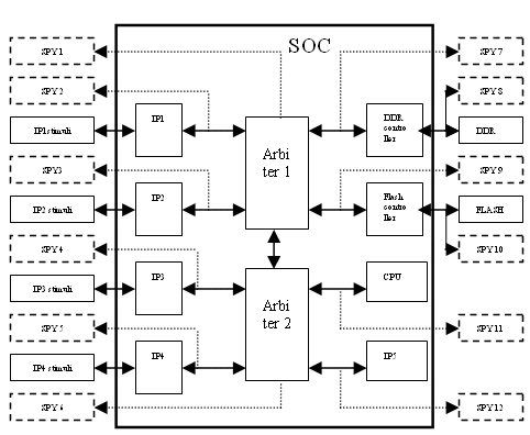
Figure 1: Typical interconnect verification platform
Test case definition:
All the use cases are already described during the product marketing definition phase (at the SoC project beginning). The first thing to do, during the interconnect architecture phase, is to rank them from the most interconnect bandwidth / latency constraining to the less constraining one.
The one which are identified as the most constraining and the most representative per use case kind will be exercised during the verification phase.
Interconnect performance verification analysis:
The interconnect performance verification (per test case run) is usually done in two parts:
- Part1: IP system constraint non violation verification.
- Part2: Interconnect running assumption verification.
Part1: Verification of each IP system constraint non violation:
This verification is done on each IP interface. During this phase, the interconnect is considered as a black box. The result of the verification is a “pass or fail”status per IP plus statistics indicating the IP running margins per test case.
Part2: Interconnect running assumption verification:
This verification is done in the interconnect by watching its internal signals around its elementary blocks (nodes, arbiters, buffers) in order to check if they are behaving as forecasted during the architecture phase. The result of the verification is a “pass or fail” status for each internal block architecture assumption plus statistics indicating interconnect running margin per test case.
Performance spy:
There are two types of performance spy (see figure 2): the “recorder spy” and the “analyser spy”.
Both spies are composed of a synthesisable state machine and a memory. The state machine processes the input signals, detects packet start and the packet end (by using condition defined by the interface and the hardware protocol). The recorder spy stores the results in the memory using the most compact format (one memory line per transaction). The memory is periodically dumped in a file during or at the end of the simulation run. The transaction sequence versus time can be regenerated by an off line post-processing software. The analyser spy only calculates statistics which are stored in the memory. The input transaction versus time cannot be regenerated by an off line post-processing software on an analyser spy dump file. Additional side band signals like FIFO level, synchronisation signal (video) might be stored in memory in order to help during recorder dump file analysis. Interconnect traffic (transaction) might by spied on initiator, target and in the interconnect (nodes, buffer, converter).

Figure 2: Recorder or analyser SPY
System corner performance measurement and verification technique:
Each IP has its own traffic which is characterized by active states and idle states. The interconnect traffic is the sum of all the IP traffics active state. System corner performance measurement and verification is achieved on long simulation run which manages as many varying delay between each IP active states. This management can be achieved by modifying one or several IP parameters to its corner value (in its valid range). Let’s take as an example a multimedia SoC including two input video sources and one video output displaying simultaneously the two incoming sources. Lets suppose that each vertical video source vertical synchronisation frequency is specified to be 60 hertz with a +/- 5% tolerance. One way to achieve a corner case system corner performance measurement for this example would be to define Vsync_source1= 63 Hz Vsync_source2= 62 Hz and Vsync_output = 63 Hz which introduces a 1 Hz frequency shift between the two input vertical synchronisations.
Emulator resource optimisation strategies:
Three emulator resource optimisation strategies can be applied depending on the expected result: the analytical approach, the statistical approach and the debug approach. The analytical approach, based on recorder spy, requires bigger memory resource and fewer gates. It provides the possibility to regenerate the IP traffic by post-processing. The memory allocation per spy can be reduced if each memory contents are periodically dumped during the simulation run. This approach is good to have a close look to one IP traffic for traffic analysis, statistics or to check one IP high level model versus its real behaviour. The statistical approach, based on analyzer spy, requires more gates and less memory usage. It is an efficient way to extract statistics of long corner cases. The debug approach is based on a recorder spy including an additional states machine which stops the simulation when a defined programmed condition is verified. The debug recorder spy memory is organized as a circular buffer.
CPU real time task constraint verification:
CPU real time task constraint can be verified by a recorder spy. This is achieved by assigning a unique number (called tag) to each real time task constraint. The CPU running software has to be programmed in such a way that the CPU writes, to a constant address in memory “constraint start address”, the tag of each real time task constraint starting. In the same way the CPU writes, to a constant address in memory “constraint end address”, the tag each real time task constraint ending. A dedicated recorder, spying the CPU interface, is parsing the addresses bus and is storing in its internal memory:
- The tag, the time and the start information when the “constraint start address” is detected.
- The tag, the time and the end information when the “constraint end address” is detected.
The “constraint start address” and “constraint end address” have to be accessed only by the CPU. This address can be easily mapped to I/O, ram or SDRAM address space.
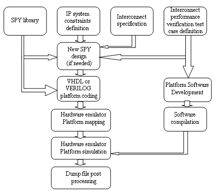
Figure 3: Hardware emulator interconnect performance verification flow chart
Hardware emulator interconnect performance verification flow:
The verification flow can be summarized as the following short list (see figure 3):
1) Get from architecture phase: test case definition and all the IP system constraints.
2) Identify any new spy characteristic related to system constraints verification needs.
3) Reuse, adapt, specify, develop and test any spies required.
4) Reuse verification testbench and add the spy to get the performance verification platform.
5) Develop and compile the software to be run by the CPU.
6) Compile the platform using the emulator compiling flow.
7) Run hardware emulator and dump output data files.
8) Post process the dump files.
9) Analyse the results.
Methodology applied to a multimedia SoC:
This methodology was used to verify the STbus interconnect performance of a complex multi source digital television SoC integrating MPEG high definition decoder and displaying simultaneously multi layered video pictures and 2D graphics (see figure 4). It embeds a 32 bits CPU + caches sharing an external DDR2 SDRAM memory with the other internal IPs. The graphics planes are built using a 2D hardware accelerator (blitter). The data exchange between IP is done using memory buffers located in the external DDR2 SDRAM. This SoC contains 52 STbus DMAs. The objective was to verify the latencies/bandwidth of each IP STbus DMA, the running margins of internal FIFOs and the DDR2 throughput efficiency ratio for several use cases.
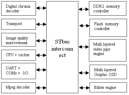
Figure 4: STMicroelectronics digital television multimedia SoC.
Recorder spy applied to STbus protocol:
The STbus protocol is based on split transactions. The STbus interface is composed of three signal sets: the control, the transaction and the service signal set. The control signal set defines when a transaction starts and stops. This set is composed of (see figure 5):
- “req”, “gnt” and “eop” (on the request path).
- “r_req”, “R_gnt” and “r_eop” (on the return path).
The transaction set is composed of data, address, opcode, byte enable and source identifier signals. The transaction set signals do not appear intentionally in figure 5 for simplification reasons. Four transaction events are represented by vertical arrows in this figure: “Ts” (packet start), “Te” (packet end), “Trs” (return packet start) and “Tre” (return packet end).
Three transaction timing are indicated too:
- “Treq” (elapsed time between “Ts” and “Te”).
- “Tidle” (elapsed time between “Te” and “Ts”).
- “Tr_req” (elapsed time between “Ts” and “Tre”).
The four events are tracked by each spy state machine. The three measured timing “Treq”, “Tidle” and “Tr_req” are stored in the internal FIFO.
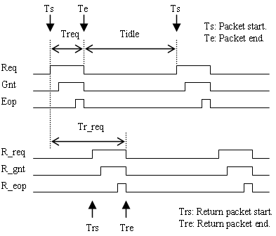
Figure 5: Simplified STbus protocol.
Spy memory structure example:
All the information related to the same STbus transaction is concatenated altogether and is stored in the recorder spy memory. Figure 6 describes a memory spy structure in which five data are stored: “treq”, “tidle”, “Tr_req”, “address” and “opcode”.
Each spy is coded in VHDL language. The number of bits used by each information kind stored in memory is defined by a generic parameter. This allows to optimize the emulator memory usage depending on the forecast spy traffic.
Note: the absolute time can be regenerated by software post processing. That is why this information is not stored in the spy memory (emulator memory space saving).
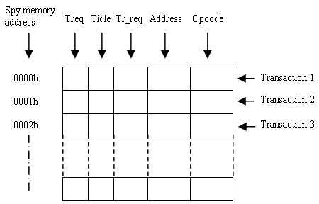
Figure 6: spy memory mapping example.
Additional spied parameters and statistics applied to dump file:
The additional usual IP parameters spied are: the STbus DMA FIFO level, input FIFO level of IP receiving a bit stream, output FIFO level of IP providing a bit stream and DDR2 throughput efficiency ratio. The statistics usually run are:
minimum (or maximum or average) calculation and histogram generation.
Figure 7 is a snapshot of one of the analysis tools developed and used during the study. Figure 8 is a return latency histogram example. Figure 9 is return latency plot example.
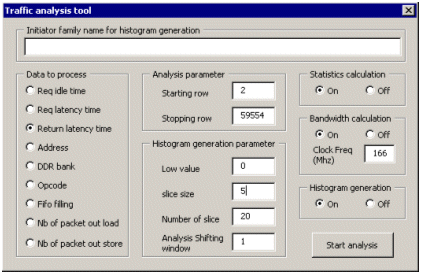
Figure 7: Analysis tool used during the study.
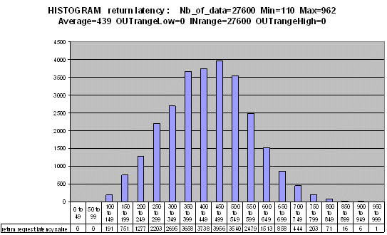
Figure 8: Return latency histogram example.
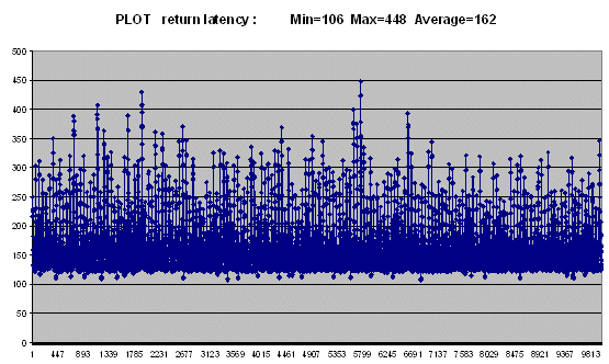
Figure 9: Return latency plot example.
SoC performance analysis results:
Three interconnect killer bugs were found during the interconnect performance verification. Each of these bugs were dead locking the overall interconnect. Hard reset was the only existing way to restart the system. Three other bugs were found:
- CPU external DDR2 writing errors with misaligned addresses.
- One over bandwidth traffic due to one IP bug.
- One IP system debug module missing in one IP.
One of the most complex parts of the study was to code and to debug both SoC hardware and software. The emulator was used in trace interactive mode during the code debug phase of this project.
The forecasted initial interconnect programming provided by the architecture team (tuned on systemC high level platform) was almost working (three FIFOs failed: they were empty when data was required). A fine tuning of this programming was done in several steps. The architecture team adapted, rerun their systemC high level platform and extracted new forecasted performance parameter per IP.
Once the discovered bugs were fixed and the interconnect programming setup was frozen, the emulator was run for the last time and each memory spy was dumped. Each IP measured parameter was compared with the expected value provided by the SoC architecture team. They were similar to the one found with high level modelling result update. The performance verification platform will be used to help for future problem understanding during the silicon validation project phase.
| Number of processed transactions per use case | Number of interconnect setting iterations | Number of killer bugs found | Number of big bug found | Medium level bug found |
| 4768200 | 6 | 3 | 1 | 2 |
Table 1: Few simulation interesting numbers.
Conclusion:
This paper described an interconnect performance verification methodology (prior to PG tape) based on a hardware emulator. This methodology was exercised on an industrial project. It improved the chances to achieve “first time right silicon” target as it put in evidence 6 bugs (including 3 killer ones). Today the verified SoC IC is functional and is in its validation phase. This methodology required the spies and the post processing tool developing. Once the spies and tools are developed, the main resource is consumed during the CPU software coding, the debugging and dump file post processing.
Related Semiconductor IP
- NPU IP Core for Mobile
- NPU IP Core for Edge
- Specialized Video Processing NPU IP
- HYPERBUS™ Memory Controller
- AV1 Video Encoder IP
Related White Papers
- An HDTV SoC Based on a Mixed Circuit-Switched / NoC Interconnect Architecture (STBus/VSTNoC)
- Performance Measurements of Synchronization Mechanisms on 16PE NOC Based Multi-Core with Dedicated Synchronization and Data NOC
- HW/SW Interface Generation Flow Based on Abstract Models of System Applications and Hardware Architectures
- Interconnect (NoC) verification in SoC design
Latest White Papers
- Ramping Up Open-Source RISC-V Cores: Assessing the Energy Efficiency of Superscalar, Out-of-Order Execution
- Transition Fixes in 3nm Multi-Voltage SoC Design
- CXL Topology-Aware and Expander-Driven Prefetching: Unlocking SSD Performance
- Breaking the Memory Bandwidth Boundary. GDDR7 IP Design Challenges & Solutions
- Automating NoC Design to Tackle Rising SoC Complexity