Skillfully Emulating a System on Chip
Shwetank Shekhar, Akshay Bisht, Maneesh Kumar Pandey
Freescale Semiconductor India Pvt. Ltd.
Abstract
Time to market is most important criteria for survival in the IC design industry. For this one should produce low cost good quality silicon in lesser time. In order to achieve this, design should be validated well before tape out in application area ecosystem and all software should be ready before silicon comes in the lab. This objective can be achieved by porting design and test environment to the emulator. This paper deals with art of skillfully porting a SoC on to emulator, architecting virtual evaluation board (EVB) and benefits of using emulation.
INTRODUCTION
In IC design, hardware emulation is the process of imitating the behavior of one or more pieces of hardware with another piece of hardware, typically a special purpose emulation system. The advantage of hardware emulation is that it combines the programming flexibilities of simulators with the performance and system integration advantages of a hardware model. Hardware emulation allows testing of ASIC designs in a full system environment operating at reduced frequencies. This offers the opportunity to debug the design more thoroughly prior to release to silicon and to start software development on the complete system much earlier in the development cycle.
Although a hardware emulation model will never operate at the same performance as the final chip design. it can operate at real time interactive system performance executing the same software as the final system. The most significant advantage of emulation over simulation is speed and its ability to operate in system environment. This paper is divided into five sections. Section I explains how to port the design on to the emulator. Section II describes how to craft the virtual Evaluation board. Section III tells about the benefits of using emulation system. Section IV highlights some of the tips that should be used for getting maximum throughput. Section V has the summary.
I. ART OF PORTING A SOC ON TO THE EMULATOR
A typical SoC consists of:
- A microcontroller, microprocessor or DSP core(s).
- Memory blocks ROM, RAM, EEPROM .FLASH
- Timing sources including oscillators and phase-locked loops.
- Peripherals including counter-timers, real-time timers and power-on reset generators.
- External interfaces including industry standards such as USB, FireWire, Ethernet, USART, SPI.
- Analog interfaces including ADCs and DACs.
- Voltage regulators and power management circuits.
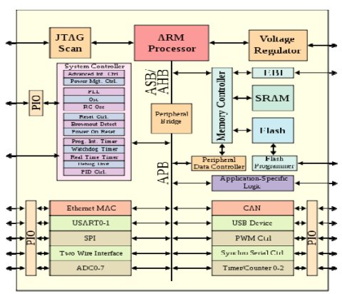
These blocks are connected by either a proprietary or industry-standard bus such as the AMBA. The SOC in the form of RTL cannot be exactly mapped to the emulator because it contains digital, analog and mixed-signal components. It is extremely important as first step to identify the analog/mixed signal components of the design and understand their behavior.

Figure: A typical SoC architecture
Next comes the resources available with the emulator. Emulators generally have domains and each domains is capable of mapping around 1million gate (this vary from vendor to vendor). Depending upon the domain available the design is modified so as to accommodate in it. The blocks which are not of interest are stubbed out.
The analog component identified such as PLL/fuses etc are replaced by corresponding stubs and memories are coded with proper coding guidelines so as to map on to the physical memories of emulator. Once these changes are done, the design in HDL form and library of the emulator is passed to the synthesizer to produce the gate level net list.
The gate level netlist is zero-delay model and contains functionality only. The stubs are empty modules and do not exhibit any behavior.
This net list with the hardware configuration, physical connection and signal preservation instructions are passed to the emulator Example: For interacting with real world, industry standard interface JTAG is used. The pin level connection for JTAG (TDI, TDO, TCK, TMS, and TRST) is done as per real world connection of emulator The clocking is done at the output of PLL.As the stubs PLL are used ,the output of PLL are defined as clock source of required frequency. By doing this clock of required frequency driven to these pins at run time.. After doing all these, net list is complied and database is created. As compilation process optimizes the proces internal nets, those of interest are preserved using keepNet instruction before compilation. On compilation it generates the ready to use emulator database.
II. ARCHITECTING VIRTUAL EVALUATION BOARD
The emulator model generated in section I of this paper is the Xerox of silicon which is used for all purpose until silicon comes in the lab. Even after silicon comes to the lab, emulation model is used for replicating all the bugs and for finding the solution of that as it provides insight into all the signals inside the design. The model generated does not have components which are available on board for running the test and prove the functionality of interfaces.
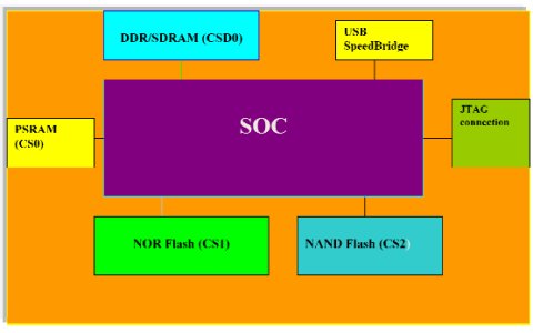
This is done by formulating the (stb) synthesizable test bench. The stb like SoC goes and sits inside the emulator providing better like speed because of no domain crossing. The stb consists of instance of the design and synthesizable model of the entire hardware component which are present on the Evaluation board. One of the samples of SOC with evaluation board component are shown below.

Figure: The Samples of SOC with Evaluation Board (EVB) Component
III. LEADING EDGE BENEFITS OF EMULATORS
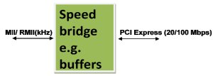
A. Using Speed Bridges actual hardware can be connected with this Box and more realistic testing can be achieved.
Emulators like Palladium works at slow clock, often in kHz because design netlist is divided into multiple cores. On the otherside debuggers which communicate via PCI Express/USB protocol is running on clocks in Mhz. Speed bridges which are basically buffe and FIFOs of suitable depth play here important role to make both work in sync.

B. Using Emulator all the test cases to be executed on silicon are made ready and debugged on emulator by either downloading via JTAG or PEX path .
This helps in Validation readiness and proves the result on very first day of silicon arrival. Before Si arrives our code is developed & tested in Pre-Si environment so that we are not developing code while Si is in our hands. This also gives faster time to market. (This is just a bonus because such code can even be developed using software emulators)
C. Debug Paths tested implicitly:
Many features like Access debug paths are not satisfactorily tested in Verification environment while emulation platform solely depends on such paths and hence such debug features are implicitly tested.
D. Less Timing Issues:
In emulator like palladium everything is sampled at one master clock (core clock, which runs typically at 188MHz in PD-III) – even asynchronous signals are sampled at this clock. So there is no concept of False/Multicycle paths. It helps us to avoid any false timing issues.
E. Faster run-time:
Run time is very fast viz. 50x, 100x and even 1000x. In verification platform Simulation run-time is very large which is really painful.
F. Patch Development for real Silicon:
Gives us opportunity to create patches for debuggers say Lauterbach,GHS so that Validation team can directly utilize them when Si arrives.
G. Critical Testing:
Critical fields like Boot areas are tested at emulation platform. This is very much necessary because we can never afford the scenario that Si has come and it is not booting only. Also SoC bandwidth issues can be uncovered easily as compared to Simulation. e.g. DFS feature. Also flash and other memory models are directly usable –as they are meant for emulation itself.
IV. SKILLFUL DEPLOYMENT OF EMULATOR TO GET MAXIMUM THROUGHPUTS
Some of the tips for effectively utilizing hardware emulator model
A. External booting with better speed
Logic inside the design determines the boot source and can be configured during power on reset. The value forced on this logic sets the boot source and core starts fetching the code from this source as soon as it comes out of reset
B. Using stubs properly for analog blocks
The blocks like PLL are completely analog in nature. This cannot be ported on to the emulator as it is not synthesizable. Without bothering too much we go for its stub model and try and do forcing of required output signals of the block. For example in case of PLL, it can be different locked outputs of the PLL and LOCK output signal itself. Other functionality of analog behavior should also be taken care while modeling stubs.
C. Initialising memories from back door
The internal memories are bulky in nature so its always good idea to map them to physical memories of the emulator so as to utilize the resources properly. Also further, in case of memories requiring initialization before usage, instead of initializing them via core memory access, we initialize them from backdoor. This saves time because core on the emulator will typically run in Khz, while using backdoor, the memory is initialized via emulator master clock (Typically in several MHz).
D. Synthesizable Monitors
With the stb mode synthesizable monitors are developed which also goes and sits inside the emulator which helps in knowing the internal state of the design from time to time or at event of interest. Even non-synthesizable statement like print can be psudeosynthesized and can be displayed at run time.
E. Automatic end of test case detection
The facility of trigger helps us in automatic end of test case completion. The trigger can be put on the condition of interest and executed at run time.
F. Visibility of signals
The real world silicon does not allow us to peep inside the silicon and probe the all the nodes of interest. When some issues come, it is very important to know the state of signal of interest. The Emulator world allow us to do this with just run time modifications.
V. SUMMARY
This paper shows that emulating the SOC is one of the excellent ways to supplement verification and validation. Walking through, we also came across the philosophy that although emulation is very beneficial but its throughput can be many times enhanced by smartly incorporating the techniques discussed hereby. The benefits outlined help us improve the time to market and debug the issues both prior to silicon and post silicon.
REFERENCES
[1] J. Bhadra et al., ''A Survey of Hybrid Techniques for Functional Verification,'' IEEE Design & Test, vol.24, no.2, 2007, pp. 112-122
[2] S. Hazelhurst et al., ''A Hybrid Verification Approach: Getting Deep into the Design,'' Proc. 39th Design Automation Conf. (DAC 02), ACM Press, 2002, pp. 111-116
[3] Incisive Enterprise Palladium Series with Incisive XE Software, http://www.cadence.com/rl/Resources/datasheets/incisive-enterprise-palladium.pdf
[4] http://www.virtutech.com/QorIQ
[5] PowerPC e500 Core Family Reference Manual, Apr 2006
[6] www.wikipedia.org
[7] Thomas A. Horvath Norman H Kreitzer “Hardware emulation of VLSI designs” Thrid Anual IEEE Proceedings, Rochester, NY, Sepetember 1990[ASIC Seminar and Exhibit, 1990].
Related Semiconductor IP
- NPU IP Core for Mobile
- NPU IP Core for Edge
- Specialized Video Processing NPU IP
- HYPERBUS™ Memory Controller
- AV1 Video Encoder IP
Related White Papers
- Power Management for Internet of Things (IoT) System on a Chip (SoC) Development
- A 24 Processors System on Chip FPGA Design with Network on Chip
- Using non-volatile memory IP in system on chip designs
- A Heuristic Energy Aware Application Mapping algorithm for Network on Chip
Latest White Papers
- Ramping Up Open-Source RISC-V Cores: Assessing the Energy Efficiency of Superscalar, Out-of-Order Execution
- Transition Fixes in 3nm Multi-Voltage SoC Design
- CXL Topology-Aware and Expander-Driven Prefetching: Unlocking SSD Performance
- Breaking the Memory Bandwidth Boundary. GDDR7 IP Design Challenges & Solutions
- Automating NoC Design to Tackle Rising SoC Complexity