Security Challenges in Embedded Designs
ABSTRACT
We present several use-cases where embedded security is a fundamental requirement. For each use-case, we list a set of security-related characteristics and translate these characteristics into security requirements. We continue by analyzing the security requirements and identifying the embedded security building blocks of each one. The information for each use-case is presented in a tabular format combined with detailed analysis, facilitating easy reference per specific use-case.
1 INTRODUCTION
Security is becoming a de-facto requirement in the embedded industry, where system integrity, content and connectivity are gaining increasing market attention. This naturally leads to security accounting for a more significant share of embedded designs cost. At the same time, with the prevalence of software there is also a need to meticulously build a design to guarantee the security, authenticity and availability properties of the overall solution.
In this paper we analyze the following use-cases where security challenges are involved:
- Software integrity protection
- Software IP protection (reverse-engineering protection, anti-cloning)
- Secure information and data logging
- Preventing use of non-original peripherals
- Secure communication
- Digital Rights Management (content protection)
- Multi-CPU System-On-Chip
For each use-case, section 2 lists the various security requirements and maps those to security building blocks. Section 3 provides a more in-depth description of each security building block.
2 USE-CASE ANALYSIS
In this section we examine various security use-cases. We begin by taking each use-case and listing the set of security-related characteristics that must be provided to support the use-case. We then take each characteristic and translate it into distinct security requirements. Finally, we take each identified security requirement and list the embedded security building blocks that must be in place in order to answer that security requirement.
2.1 SOFTWARE INTEGRITY PROTECTION
Software resides on a permanent external storage device (e.g. external flash), which is relatively easy to access by simple off-the-shelf tools. An attacker can replace parts of the software image or the entire software image on external storage, causing the CPU to execute software which was not originally provided or approved by the manufacturer. Such software modifications can cause a wide range of undesired system behavior. The result can vary from simple loss of revenue to hazardous unintended behavior malfunctions.
The manufacturer introduces software to the system at two distinct occasions. During manufacturing, the manufacturer introduces software to the device by programming the flash memory. At a later stage, the manufacturer can update the software image on flash by means of a secure software update session. The requirement is to maintain the integrity of the manufacturer software on both occasions and this is done by assigning a unique signature to the manufacturer’s software.
The unique signature over the software image is based on public key cryptography. A unique digest (e.g. hash) value is calculated over the software image and the manufacturer uses its private key to sign the software image hash. The software image and its signature are then loaded to the system during system manufacturing, along with the associated manufacturer’s public key. Whenever there is a need to authenticate the software image, a digest of the software image is calculated and the public key is used to authenticate the private-key-generated signature. Any piece of software not signed by the manufacturer is detectable at a later stage as non-authentic software.
Secure Key Storage must store the public key and protect it against modifications, otherwise the authentication mechanism can be easily broken. An attacker interested in injecting a new software image can randomly create a new private-public key pair. The attacker then uses the private key to sign the new software image (in the same manner as the manufacturer does) and loads the new software image, new signature and the matching new public key to the system. During such an attack, the authentication scheme passes successfully, as the public key used for authentication matches the private key which was used to sign the software image. This attack is foiled by storing the public key in a secure key storage area. This prevents an attacker from loading a different public key to the device.
There are many options for secure manufacturer public key storage. The public key can be stored in on-chip ROM – there is a clear advantage that the public key cannot be replaced, but also the disadvantage of lack of flexibility – all systems have the same public key, meaning that all manufacturers must use the same private key to sign the software image. A second option is to store the public key in on-chip One-Time-Programmable (OTP) technology – the advantage here is flexibility, where each chip can have a different public key, but carries the disadvantage of silicon area cost of a large number of OTP bits. A remedy for that is a third option, where the public key is stored on external flash, but a hash value of the public key is stored in on-chip OTP – maintains the solution flexibility but dramatically reduce the number of required OTP bits.
Detection is carried out primarily by a Secure Boot function at boot time – during system boot the software image is authenticated versus its signature. The Secure Boot function is an on-chip ROM-based procedure, which carries the above-mentioned authentication scheme. The reason the function must be ROM-based is so that an attacker cannot intercept the procedure and so that authentication is always carried during boot, bringing the system to a known and trusted starting point. Whenever the manufacturer wishes to update the software image on flash, best practice is to do so at Secure Boot time, because at this point in time the system is at a known state for the update to commence.
An attacker is also likely to attempt to modify the software while the system is running. There is a need for Run-Time Integrity Checking (RTIC) capability, which periodically authenticates the software image post-boot, either directly on XIP NOR flash or on external RAM for NAND flash implementations. RTIC operation is similar to Secure Boot operation, with slight modifications to accommodate runtime changes. RTIC function must run in a Secure Execution Environment (SEE) with its own dedicated RAM, where it is guaranteed that the RTIC functionality has not been tampered with by an attacker. Considering that an attacker can attempt to modify the RTIC code or the procedure that calls the RTIC in the first place, it is evident that the RTIC must run in an SEE. The SEE must also maintain a Secure Timer, which periodically triggers the RTIC function.
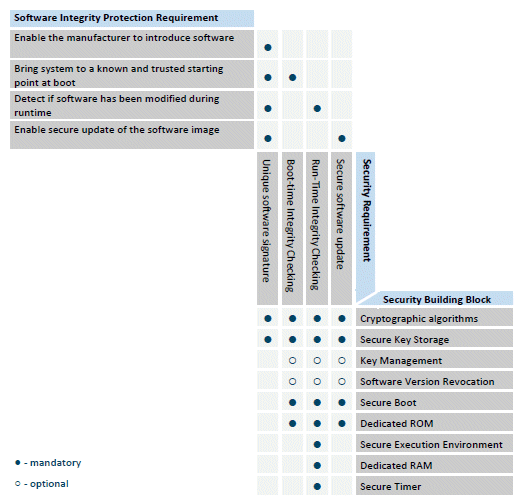
Optional mechanisms helpful for software integrity protection include a mechanism for Key Management, in situations where more than one private-public key pairs need to be supported (for example, to enable private-public key pair revocation for stolen keys). A Software Version Revocation mechanism is important for long-lived systems, where the manufacturer may want to advance the system to a new version of the software and prevent roll-back to an older version. In such a case a software version counter is tied as part of the Secure Boot signature, enabling this mechanism.
2.2 SOFTWARE IP PROTECTION
The software code image that the CPU executes may contain valuable IP and know-how, which the device manufacturer wishes to protect. Protection is required both against cloning of the system (anti-cloning protection), as well as against reverse-engineering of the software. Cloning provides the attacker with the ability to create a copy of the device, which would result in loss of revenue to the original manufacturer who cannot sell its own device. Reverse-engineering carries an even greater penalty, as the attacker is gaining access to the manufacturer knowledge base, and is able to build many competing devices, not just the specific device where the IP was stolen from.
As mentioned, the software resides on an external storage device, which is relatively easy to access. An attacker can copy the software image, as well as reverse-engineer the software to reveal the manufacturer’s ideas and know-how. A starting point for protecting the software image is by means of code encryption, such that the attacker doesn’t have access to the encryption key. Access must also be prevented to the plain code itself once decrypted, when it is located in on-chip RAM.
The encryption key used to encrypt the software image must be stored using a Secure Key Storage mechanism. At the basic level, key storage can be with on-chip ROM (less flexible) or One-Time-Programmable (OTP) bits. Optionally, for more advanced systems which handle a large number of keys, keys are better handled using a full Secure Storage solution based on a Unique Secret Key, with a Key Management function to handle all key material (see section 3.2)
Finally, the code encryption key must be loaded into the system, as well as the encrypted software image. Key material is loaded using a Provisioning mechanism. Provisioning refers to the manufacturer’s ability to load data into the system in a secure manner, even when manufacturing is performed in unsecure locations. Provisioning is necessary both for loading the encryption key as well as loading the code image. The code image can be pre-encrypted and loaded already encrypted to the flash, or loaded plain to the flash and encrypted during the system’s first boot.
Once the image is ready encrypted on flash, there is a need for fast on-the-fly code decryption. On-the-fly refers to the capability to decrypt the code as it is being read from external storage and into on-chip RAM. Fast decryption is required in order to add minimal stalls to the system performance. As with the code encryption phase, the encryption key must be available for the decryption engine.
The manufacturer can update the software image on flash at any point in time by means of a software update session. This requirement has been discussed in the previous section for when the update software already arrives encrypted. Otherwise, the only difference here is that the update session includes an encryption phase.
An attacker might also try to extract IP by probing internal RAM, where the code resides in plain form, using the chip JTAG interface. The requirement here is to provide JTAG debug interface protection. Debug port protection is carried out by a dedicated Secure JTAG unit, which resides on the JTAG entry point. Whenever a technician is interested in debugging the chip, the technician uses the debug tool to ask the on-chip Secure JTAG unit to send a challenge (based on a cryptographic scheme). The challenge is received by the debug tool and if it is an authorized debug tool then the debug tool is able to create the appropriate response to authenticate itself. The secret for the authentication protocol must be provisioned to the chip at an earlier stage, similar to key provisioning described above.
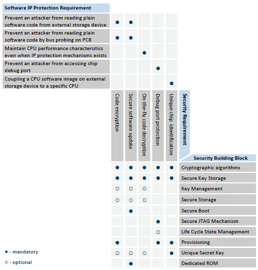
Once authenticated, the Secure JTAG unit opens the JTAG chains and enables debugging of the chip. An attacker would have a hard time accessing JTAG chains and internal RAM when such a mechanism is in place.
Optionally, the Secure JTAG can rely on a Life Cycle State Mechanism. The Life Cycle State mechanism is a one-way function which indicates the current system state (e.g. development, production, user, end-of-life, etc). When the system is in development, a developer would not want to perform the challenge-response procedure every time. The Secure JTAG mechanism can hook to the Life Cycle State indication and since development stage is carried out in a secure environment, disable the JTAG protection.
Even if the code image is encrypted, the code image is not tied to a single chip or a single CPU. Therefore, cloning the system is possible by copying the code image as is and running it on an identical chip over the cloned system. Since the cloned chip CPU knows how to read the encrypted image, cloning at the system level is possible. The attacker doesn’t understand the code that is executing on the CPU, but gets the expected behavior out of the CPU. The solution here is to use a Unique Secret Key per a specific chip and tie the chip’s code encryption to this unique key.
2.3 SECURE INFORMATION AND DATA LOGGING
Secure logging of information and data is an essential system property. Some pieces of information require only protection against modification (e.g. identity), while other items in the database also require protection against reading (e.g. private keys). Implications of not enforcing access restrictions on such pieces of information range from commercial fraud to legal repercussions.
The basic requirement for secure information logging is to provide a Secure Storage database. The Secure Storage is based on a unique secret key stored by a Secure Key Storage mechanism and cryptographic algorithms which provide the security infrastructure, which will be discussed shortly.
Throughout this paper we outline mechanisms which are based on secret encryption keys. Each such key can be stored using on-chip ROM or OTP bits, although such solutions are either inflexible (ROM) or costly in terms of OTP silicon space. The system approach to alleviate the large on-chip storage requirement is to use a Secure Storage database, which is based on a single on-chip unique secret key. The Secure Storage database can store an unlimited number of keys or any other data items. Secure Storage creates a hierarchical approach, where one on-chip key protects a large number of off-chip keys.
Maintaining high-reliability of the underlying database is of key importance. Two features providing for high-reliability are the ability of the database to correct itself against unexpected errors. For example, unexpected power-loss can render the database at an unknown state. An application error can also have a similar effect, resulting in a corrupted database. Protection against unexpected errors can be accomplished by journaling methods, where a journal of database transactions is maintained. Such journaling methods can facilitate database roll-back capability, as well as unexpected power-down recovery. Even when using such techniques, it is important to remember that we are discussing a secure database, where the database is constantly protected for its integrity. Every update to the database also requires updating the integrity mechanisms.
Attacks on the database can occur off-line or on-line. An off-line attack involves reading or modifying the database on the external storage device (most likely flash) while the system is powered-down. In order to prevent reading database items, the database should employ encryption methods to provide data confidentiality. In order to prevent modifications of database items, the database should employ digest methods to provide data integrity. Both the confidentiality and the integrity of the database are based on encryption keys and therefore require Secure Key Storage capability. If the attacker doesn’t know the encryption keys, the attacker cannot decipher the database items, nor break their integrity without being detected. In order to raise the security barrier further, it is best to use hardware-based key storage techniques (e.g. OTP), which provide significant improvement in the level of security compared to software-based techniques.
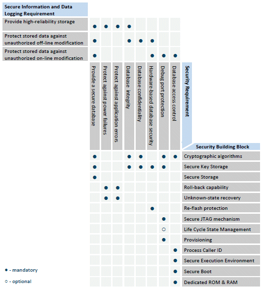
In order to prevent on-line database modification, a secure JTAG mechanism must be employed. This mechanism has been discussed earlier in this paper. Furthermore, the software handling the Secure Storage database must be isolated and executed in a Secure Execution Environment (SEE) with its own Secure Boot function and dedicated ROM & RAM, so that all key material is handled in a trusted compartment. The Secure Storage database should be integrated with the operating system, so that better access control is available. In particular, using cryptographic methods a unique process Caller ID indication can be provided per each system process, enabling the Secure Storage software to identify the various processes which are asking for database services.
Finally, even the Secure Storage database is prone to re-flash attacks. Re-flash attacks refer to the attacker’s ability to save a copy of the database now and at a later point in time overwrite the database with the saved copy. Because the saved copy is a legal copy of the database (passes all integrity checks), the attacker is able to bring the system to a known previous state. The solution to re-flash attacks involves adding a secure timestamp to the database integrity. Adding such a secure timestamp requires some on-chip Non-Volatile-Memory (NVM) counter, which is increased every-so-often and added as part of the Secure Storage database integrity.
2.4 PREVENT USE OF NON-ORIGINAL PERIPHERALS
Loss of revenue occurs when non-original peripherals are used instead of authorized parts. The manufacturer is interested in preventing such a scenario and limiting the system to work only with authorized components.
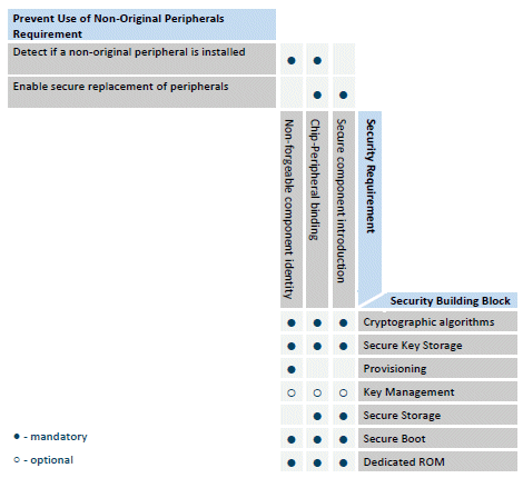
In order to detect non-original peripherals, each peripheral must have a non-forgeable identity. The identity doesn’t necessarily have to be unique per a specific peripheral – a batch of peripheral components can have the same signature (for example, to ease inventory control). In order to establish peripheral attestation, one needs to securely provision a secret in the original peripheral. Example secrets can be the peripheral manufacturer’s private key, or a shared secret. The matching public key or shared secret can then be used to uniquely identify the peripheral. The secret must be kept securely in the original peripheral, such that it is not possible to easily extract it.
Peripheral authentication is one-way, in the sense that the chip is authenticating the peripheral and not vice versa. When the chip wishes to identify the peripheral, the chip sends a challenge to the peripheral. The original peripheral is able to use its provisioned secret to provide a response back to the chip. The chip can then verify the response with its provisioned information. The chip must keep the secret in Secure Storage, so an attacker cannot replace the secret (as before, more complex Key Management schemes can be used if the total system key count is high). If an attacker is able to replace the secret, then whenever the attacker’s non-original peripheral is embedded in a system, the attacker provides a hack to replace the matching secret in the chip storage, thus enabling the non-original peripheral to work.
Installing a new peripheral relies on the non-forgeable identification of the component, as well as the algorithm which is unknown to the attacker. The process of binding a peripheral to a chip involves the chip authenticating the peripheral, as well as registering its identification and possibly other parameters in the chip’s Secure Storage database.
Secure Boot running from on-chip ROM is mandatory for detecting non-original peripherals. Only when the system is at a known and trusted starting point is it possible to verify all connected components and take action in case of detecting a non-original peripheral.
It is possible to raise the security bar by performing two-way authentication, where the original peripheral is also authenticating the chip. This requires similar security logic to be implemented at the peripheral side and is likely to be commercially applicable only for high-end components.
2.5 SECURE COMMUNICATION
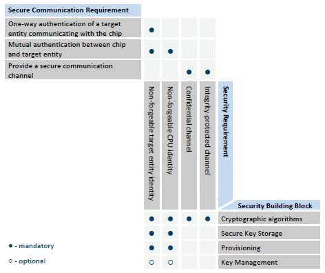
The purpose of secure communication is to prevent an attacker from masquerading and sending false or misleading data to the chip. Secure communication can also enable one-way or mutual authentication between the chip and other entities.
When the chip communicates with a target entity, the chip primarily needs to ascertain the identity of the entity. This requires the entity to have a non-forgeable identity. Utilizing public key cryptography methods would provide the most effective way to address this requirement – the target entity holds a private key and the chip is provisioned with the matching public key. Using the public key, the chip is then able to authenticate the target entity. The public key must be kept in a Secure Key Storage, otherwise the attacker might replace it and lead the chip to believe it is communicating with a different entity.
The previous paragraph dealt with one-way authentication, where the chip authenticates that target entity. Certain use-cases would require mutual authentication, where the target entity also needs to authenticate the chip. Such mutual authentication is easily achieved in the same manner as just described, using a second private-public key pair: this time the chip holds the private key and the target entity holds the matching public key. A Key Management mechanism can optionally assist in key handling if the system holds a large number of keys.
Finally, there is a need to establish a secure communication channel, which means that data is encrypted for confidentiality and also integrity-protected. Various security protocols are useful here, including Diffie-Hellman if there is a need for secure key agreement.
2.6 DIGITAL RIGHTS MANAGEMENT
Digital Rights Management (DRM) is mandatory today in places where valuable content exists. The device is responsible for enforcing the content access rights, and is liable for commercial loss if broken. Security aspects of DRM include, amongst other things, enforcement of usage rights, key protection as well as content decryption.
DRM content arrives encrypted. Therefore, the DRM process concludes when the system obtains the content decryption key. Once the content decryption key is available, it is possible to decrypt the protected content. The security aspects of the content decryption process involve Secure Storage of the content decryption key when not used, using some Key Management functions to retrieve the content decryption key and applying the appropriate cryptographic algorithm to the content. At any point in time, all key material must be protected from potential attackers (for example, by using a hardware-based decryption engine, where any key material never leaves the hardware environment).
DRM Key material protection is required not only for the content decryption key, but also for any other DRM-related keys. An example of such key material is the device key, which is used by the licensing entity to uniquely identify the device. Key material protection involves not only using a Secure Storage Secure Communication mechanism, but also a secure provisioning solution, which is able to securely inject the device key into the system.
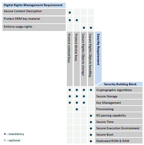
At its basis, DRM deals with usage rights enforcement, as appearing in Rights Objects (ROs). Working with ROs has two security-related aspects – RO storage and RO handling. First, ROs must be stored securely in a Secure Storage database. Since a DRM-enabled system can hold numerous ROs, a full-blown database must be used, enabling unlimited number of data items to be stored securely with an efficient search mechanism. Secure Storage is mandatory (as opposed to regular storage), since ROs contain enforcement parameters, such as the remaining usage counter, or the expiration date. Second, ROs must be handled in a Secure Execution Environment (SEE). The SEE must handle two aspects of security – parsing the RO correctly and keeping track of secure time. Secure RO parsing is necessary as some RO fields are not fail-safe in nature. For example, OMA DRM ROs have the time constraint in plain XML format – an attacker can simply erase the appropriate XML lines and the time constraint disappears. Secure Time is necessary in order to be able to enforce any time-related usage.
2.7 MULTI-CPU SYSTEM-ON-CHIP
A System-on-Chip (SoC) is not limited to hosting just one CPU. The use-case discussed here is of a single central security engine that provides security services to multiple CPUs. When consolidating several CPUs together into a single SoC, it is important to provide a framework for mutual-distrust between the CPUs, such that one CPU cannot compromise the security of other CPUs.
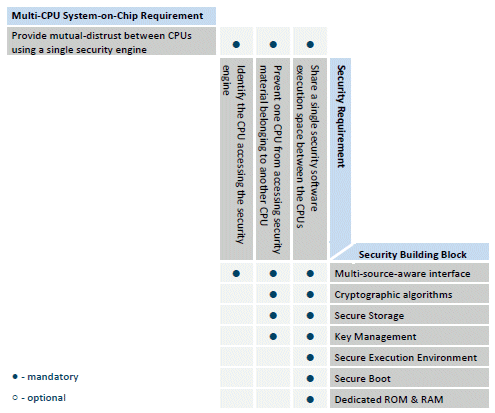
The first step to establish distrust between CPUs is to enable the central security engine to distinguish which CPU is addressing it at any point in time. Identification must be robust and therefore should be based on hardware signals. As an example, many advanced bus architectures today provide the transaction source indication as an integrated part of the transaction, using side-band signals.
Once the CPU accessing the central security engine is identified, there is a need to prevent that CPU from accessing security-related material belonging to another CPU. Assuming lack of dedicated RAM per each CPU, the best method to provide such access separation is by means of cryptography. At system initialization, a Key Management unit assigns a dedicated random key to each CPU. These keys are kept protected using a Secure Storage mechanism. All security related material belonging to a given CPU is encrypted using its dedicated random key and is therefore inaccessible to other CPUs.
Additional mechanisms can be added on top of the basic separation mechanism just described. For example, if two CPUs need to share information in a secure manner, then a random inter-CPU communication key can be defined, which is accessible only to the two CPUs.
If more than one CPU needs to execute security related software, then it makes sense to use a central security software execution space. The execution space is based on a Secure Execution Environment (SEE) with its own dedicated ROM for Secure Boot and dedicated RAM for software execution. The SEE, being trusted by all CPUs, has access to all key material and is therefore able to support all CPUs without compromising each CPU’s security.
3 SECURITY BUILDING BLOCKS
In this section we provide details on some of the security building blocks that were identified in section 2.
3.1 CRYPTOGRAPHIC ALGORITHMS
Cryptographic algorithms are an essential building block of a robust security solution. Generally speaking two types of algorithms are utilized: symmetric cryptography and public key cryptography. Symmetric algorithms are used mainly for data encryption and data integrity, due to their high performance characteristic. Public key cryptography is used mainly for key exchange, attestation and authentication, due to its asymmetric nature and lower performance characteristics.
The Advanced Encryption Standard (AES) is a secure choice for a symmetric block cipher. The Secure Hash Algorithm (SHA) is the industry accepted block hashing algorithm. For public key cryptography, Rivest-Shamir-Adleman (RSA) is the most widespread algorithm, with Elliptic-Curve-Cryptography (ECC) gaining market traction, due to its improved performance-to-key-size ratio.
Systems can instantiate a cryptographic algorithm either as a hardware cryptographic engine or a software cryptographic engine. The advantages of a hardware-based engine are security and obviously faster performance. Security is more robust as key material is only present in hardware registers inaccessible to the software and never in relatively easy-to-access RAM. The disadvantage of a hardware-based engine is the silicon footprint. The advantages of a software-based engine is flexibility, while the downside is that a software-based engine takes considerable MIPS from the processor on which it is running, which is likely to need the computation power for other tasks.
3.2 SECURE STORAGE
Secure Storage is as basic a building block as the cryptographic algorithms. Cryptographic algorithms require keys as their basis for operation. Since the algorithms are published and known to all, including to potential attackers, protecting the secrecy of the key is an important issue for security. Secure Storage essentially deals with protecting access to keys and other pieces of data. Secure Storage also needs to be persistent, such that items are not lost during power cycles.
Examples of persistent storage are on-chip ROM memory, on-chip One-Time-Programmable (OTP) technology, as well as off-chip flash memory. On-chip storage has the advantage in that it can be more easily hooked to the security solution, while having the disadvantage of larger silicon footprint and lack of flexibility. Off-chip storage is very flexible, but requires employing more careful access control schemes. If more than a few keys require protection, then on-chip solutions quickly become unpractical and it’s best to use off-chip storage.
The first step in order to protect access to plain keys (or any other data items) on an external flash is to encrypt the keys prior to their storage. Such encryption is able to thwart basic attacks techniques of simply reading flash content or probing the bus signals passing between the flash chip and the CPU chip. Adding integrity protection for each key also prevents the attacker from utilizing replacement attacks.
Once the encrypted key is within the chip boundary, it is still prone to attacks. The basic question is which root key is used to encrypt all other keys residing in the Secure Storage database. The best practice here is to use a hardware-based solution for this root key: on-chip OTP bits. Using OTP bits provides the chip manufacturer with the flexibility to program a different random root key for each and every chip, which in turn leads to a Secure Storage database which is encrypted with a different key for every chip. The other option is to use a software-based root key, where the root key is stored somewhere in the software image on flash.
Breaking a Secure Storage database with a root key that is hardware-based requires the attacker to decap the chip and attempt to read the OTP value. Such an attack is not scalable, since the attacker needs to repeat the same attack for every chip. On the other hand, using a software-based root key provides a scalable attack pattern: once an attacker manages to analyze the software image and find the root key, the attacker is able to easily distribute the attack and reveal every root key in every chip.
Assuming that the root key is indeed hardware based, it should still be used in a secure manner. The best practice here is to use a dedicated hardware module which reads the root key directly from OTP bits and decrypts encrypted keys fetched from the Secure Storage on flash. Using such a dedicated hardware module means that the root key is contained in a defined hardware block and is never exposed in more attack-prone locations such as CPU RAMs. The dedicated hardware module can range from a single dedicated engine up to a full Secure Execution Environment – depending on the type of assets available on the chip.
The final aspect of access protection is to limit the CPU applications which are accessing Secure Storage keys. A robust Secure Storage solution is able to use cryptographic measures to uniquely identify each CPU application and ascertain whether this application is allowed to use the root key in order to decrypt Secure Storage data.
Additional features are required in order to provide a complete Secure Storage solution. Primarily, the Secure Storage database should be able to recover from unexpected power-loss as well as unexpected application errors – neither one should render the database useless. Fast search capability is required when handling a large database, providing reasonable performance characteristics. Smart utilization of buffers is essential in order to decrease flash wear out, both for reads and writes. Finally, as discussed in section 2.3, the Secure Storage database is prone to re-flash attacks. The solution to re-flash attacks involves adding a secure timestamp to the database integrity.
3.3 SECURE BOOT
The purpose of Secure Boot is to bring the system to a known and trusted state. Because CPU software image resides as plaintext (i.e. unencrypted) on external flash, an attacker can easily modify the code and cause the CPU to run code which was not intended to run.
Secure Boot, as described in section 2.1, works by calculating a hash value of the software image. The hash value is then signed using the software manufacturer private key, to create a unique signature which an attacker cannot forge without access to the private key. The unique signature is then loaded to the flash alongside the software image. The software manufacturer’s public key is also provisioned to the system.
The Secure Boot routine is a ROM-based routine which performs the following steps at boot time: reads the software image from flash, calculates the hash value of the software image and uses the software manufacturer’s public key to verify that the new hash just calculated matches the old hash present on flash and signed by the software manufacturer’s private key. Even a single bit modification of the software image will lead to a different hash and as a result will lead to Secure Boot failure. As mentioned in section 2.1, the Secure Boot function must be ROM-based, so that an attacker cannot intercept the procedure.
Additional features are required in order to provide a complete Secure Boot solution. These include the ability for software update at any point in time. Given that the software is correctly signed with the software manufacturer private key, the Secure Boot routine should pass successfully. If the software image is constructed of several components, the Secure Boot routine should be able to accommodate multiple software vendors and multiple keys used to sign the image. If a private key has been compromised, the Secure Boot routine should support revocation of a compromised private key and discard the appropriate public key. Finally, a Software Version Revocation mechanism is able to advance the system to a new version of the software image and prevent roll-back to an older version.
3.4 SECURE JTAG
The JTAG interface is a debugging interface for chips. It is used primarily during development and manufacturing, but also used to help debug errors that are found in the course of the lifetime of the system.
The JTAG interface is potentially exploitable by attackers, who can try to read internal registers or memories. A current widespread solution is to disable JTAG completely when the system leaves the manufacturer’s facility, by physically disconnecting the JTAG lines. Of course this solution is secure, but prevents the manufacturer from any future debug capability.
It is possible to leave the JTAG interface active and protect it using a Secure JTAG mechanism. Whenever a debug tool is interfacing the chip through the JTAG interface, the Secure JTAG mechanism issues a challenge-response protocol with the debug tool, as was described in section 2.2. The purpose of the protocol is to authenticate the debug tool attempting access to chip internal JTAG chains and is based on some shared secret between the chip and the manufacturer who controls the debug tools. The shared secret needs to be provisioned to the chip during manufacturing and be kept securely.
An additional feature required in order to provide a flexible Secure JTAG solution is a Life Cycle State Mechanism, which enables the Secure JTAG mechanism to know whether the chip is currently in development (and hence no need to enforce the access policy on the JTAG interface), or already deployed in the field (at which time the JTAG access policy is enforced).
3.5 SECURE EXECUTION ENVIRONMENT
Throughout this paper we have discussed several use-cases which require a Secure Execution Environment (SEE). An SEE is a processing unit which is capable of executing applications in a protected manner, meaning the attacks originating from outside the SEE cannot tamper with code and data belonging to the SEE.
The first building block of an SEE is of course a secure processor – either a dedicated processor or one capable of supporting a secure mode, which is hardware compartmentalized from the non-secure mode. Utilizing a dedicated processor has the advantage of ease of separation as well as offloading the main processor from handling security tasks. The disadvantage of a dedicated processor is the increase in silicon footprint. The advantages of using one processor with two compartments is exploiting remaining MIPS if available, while the disadvantages include the need for better system design, loss of MIPS, and harder proof of security robustness.
The second building block is secure code and data memory – most likely dedicated on-chip RAMs. It is important to remember that whenever code is present outside the SEE memory it should be integrity protected against modifications (and possibly protected for confidentiality by means of encryption if required). Whenever data is present outside the SEE memory it should be protected both for confidentiality and for integrity.
Using dedicated memories has the disadvantage of increasing the chip silicon footprint. In order to reach the optimal memory size, careful analysis needs to be performed over all security applications and their total memory requirement aggregated to reach the size of necessary on-chip memory. A better approach is to use secure cache mechanisms. Secure caches offer an unlimited code and data spaces, supporting a virtually unlimited number of security applications, while maintaining a constant and small on-chip dedicated memories (for example, 8Kbyte for I-cache, 8Kbyte for D-cache). Secure cache mechanisms keep the SEE code and data secure on external RAM and fetch the necessary code and data as the security application is running, accommodating on-the-fly decryption and integrity verification. As mentioned above, whenever code or data are available outside the SEE it should be adequately protected.
4 SUMMARY
In this paper we have looked at several use-cases that require security foundations. For each use-case we defined the set of features that involve security and from these feature we derived the security requirements. Analyzing each security requirement we identified the embedded security building blocks. The use-case analysis was also presented in a tabular format, showing the clear flow from requirements to building blocks. Finally, several security buildings block were discussed to some extent, highlighting characteristics which are of importance to the system designer.
Related Semiconductor IP
- NPU IP Core for Mobile
- MSP7-32 MACsec IP core for FPGA or ASIC
- UHF RFID tag IP with 3.6kBit EEPROM and -18dBm sensitivity
- NPU IP Core for Edge
- Specialized Video Processing NPU IP
Related White Papers
- Deciphering phone and embedded security - Part 4: Ideal platform for next-generation embedded devices
- Memory solution addressing power and security problems in embedded designs
- Open-source hardware for embedded security
- Intellectual property security: A challenge for embedded systems developers
Latest White Papers
- Ramping Up Open-Source RISC-V Cores: Assessing the Energy Efficiency of Superscalar, Out-of-Order Execution
- Transition Fixes in 3nm Multi-Voltage SoC Design
- CXL Topology-Aware and Expander-Driven Prefetching: Unlocking SSD Performance
- Breaking the Memory Bandwidth Boundary. GDDR7 IP Design Challenges & Solutions
- Automating NoC Design to Tackle Rising SoC Complexity