Challenges in developing a reusable IP core USB OTG IP case study
Bangalore India
Abstract:
The idea of having Reusable IP cores is to accelerate the development of a product (SoC) by using proven IP core or design blocks that are already developed so that design & development tasks are reduced or even eliminated. The result of design reuse is that the large parts of a large SoC design can be done very rapidly, instead of designing the individual components from scratch. However there is no single answer to the question: "How much do I have to invest to make an IP reusable?" This paper describes the typical issues faced in developing a reusable IP core intended to be used in SoC applications. The methodology followed in developing a USB OTG IP core is taken as an example. How the issues are addressed in the development of the USB OTG core is explained. Lessons learned during the above process are summarized towards the end of paper.
1. Introduction
When we think about the idea of having a reusable IP core, the following typical questions used to come to our mind. “What additional work must be done to make an IP reusable?” “Is it better to create the reusable IP from scratch or take a stand-alone design and make it reusable?” “If an existing IP is made reusable, then does it take more effort to make an IP reusable than to design a new IP?” And “after how many reuses does the investment pay back?”
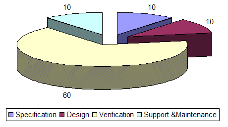
Figure 1. Effort distribution in reusable IP core development
Typical effort distribution in the development of a reusable IP core is shown in figure [1]. In the following sections (Section 2,3,4 and 5), we will walk through the different phases of a typical IP core development. In section 6 we will look into the details of USB OTG IP core development as such.
2. Specification Creation
For a re-usable IP core this phase is very critical. The term "re-usability" needs to be carefully addressed here. There are two levels of requirements applicable for the IP.
- Functional requirements coming from the driving standard and specifications
- SoC platform requirements
: This is an easy one to address, provided the driving standards and reqirements are mature.
SoC platform requirements: These requirements may vary between SoC’s, and are difficult to address across a broad spectrum of SoC platforms. However, a more critical analysis shows that, in typical embedded SoC platforms, few requirements can be common across SoC’s. These could be:
Bandwidth requirements: It is always preferable to have an IP with DMA capabilities. This will reduce the load on the host CPU.
Clocking and Power Management requirements: Separate the IP core specific clocks from the SoC bus interface clock. This can be done by using system bus adapters, (with clock crossing) between IP and SoC. The advantages are,
- The IP function becomes more or less independent of system bus clock.
- Provide freedom for the SoC integrator in choosing the system bus clock.
- Easy to implement power management scheme
: The number and frequency of interrupts from the IP and the latency requirements are to be considered here. It is always preferable to have less number of interrupts from the IP. The latency requirements may range from a few microseconds to of the order of few milliseconds.
Reset: It is still a debatable question on whether to support asynchronous reset flip-flops or synchronous reset flip-flops. If the IP employs lots of clock gating, then asynchronous reset is preferred.
Control and data path: It is better to have separate control & data path interface for the IP. This will give flexibility & freedom for the SoC integrator in connecting the IP to either a single or separate system bus. Typical SoC implementation may have all DMA agents on one bus, and all control paths connected to the processor bus.
External interface: The external interface referred here is the IP-specific interface pins coming out of the SoC. From a SoC point of view, it is always preferable to have digital signals coming out of the IP. This means at the SoC level there is a possibility to multiplex the functional pins to reduce the pin count. However, from the functional point of view of an IP, the above requirements may be difficult to meet. For example, a USB core can never work without an analog transceiver. The best way to address this, is by creating good documentation on how the digital portion of the core gets integrated with the analog part, and to the possible extent align with a governing standard, if applicable.
IP configurability: Expanding the functionality refers to parameterization or the introduction of new features. One has to be aware that investment in verification will increase exponentially and not linearly if functionality is expanded. Adding new deliverables refers to a complete and formalized documentation (for optimal know-how transfer) or additional deliverables such as new views - for example, a behavioural model. This means IP configuration need to be carefully examined. Typical use cases are to be discussed within the SoC community and a decision to taken on what configurations is important and viable.
3. Design & development
Here there are three issues to be taken care.
The first one is to design in such a way that the core functional requirements coming from the driving standard/specifications are separated out from the SoC platform requirements.
The second one is that the IP is to be designed according to a set of design rules that enable the IP to be used seamlessly with typical design flows used across SoC. This makes the implementation of the core very straightforward. This calls for a set of guidelines like, coding structures, views provided for the IP etc.
The third and the most important aspect are on design reuse within the IP development itself. Most of the time the reusable IP designs are not created from scratch. This means a stand-alone design is taken, and sufficient changes are made to make it a reusable IP core. The major advantage of reusing a design would be that the risky part has already been done and the core is proven in the original application. If the design reuse is employed within the IP development itself, then the following steps are a must.
Assess the state of the design database so that an estimate of work involved in converting the database to a reusable one can be prepared. The most important task is to ensure that the existing functional verification of the design is of high enough quality, if it is not then extra verification will have to be done. Since most legacy design is done on a one-off basis for one application, this tends to be the most serious problem when reusing a design. Other factors to be considered here are the suitability of database with typical tool flow, existing documentation, and good support from the original design team.
Sufficient time must be scheduled to understand the code, to determine the parameters to test the IP, to write the test bench, where needed, and to complete the verification.
4. Verification
Several approaches are possible for in-depth verification of IP. Definition of test scenarios to simulate as many operating modes as possible has to be accommodated in a reasonable time. The confidence level will increase as the overall simulation matures. Use of code coverage tools can be tried during simulation. Silicon validation, such as FPGA implementation or the production of test chips, will allow more-extensive verification because nearly real-time simulations are performed and, hence, the overall simulation time will decrease significantly.
However the biggest problem in IP verification is the lack of a standardised methodology. Each design task, from system architecting to prototyping, has its own verification stage to go along with it. Today each design task uses its own isolated verification environment with very little reuse between the tasks. For example the block level test environment used become useless when moving to the sub system level, and the subsystem level test bench may become use less when moving to system level. The result is a slow, grossly inefficient overall methodology.
The verification problem is becoming more difficult when moving to the IP-SoC integration. Most of today’s SoC designs include many IP blocks, each of which might have performed extensive verification. Unfortunately, the IP integrator cannot infer any useful information from the IP verification environment, because of the non-standardized and incompatible verification environments and approaches used between the IP and SoC. At the other end of the design process, a SoC design team provides little information to the IP creator on how they would like to integrate the IP to their SoC. Given that the majority of overall design time is spent in functional verification, these have become major problems.
The following three critical areas must be addressed by anyone providing IP for SoC integration.
- Perform thorough standalone functional verification of the IP
- Provide stand alone verification environment for the IP (This enables the IP user to perform out of box testing)
- Supply a portable verification environment and test cases (for e.g. ‘C’ test cases, and complete HDL test environment) along with the IP that enables the SoC integrator to verify the IP in the context of the full SoC.
Support and maintenance is something extra required for a reusable core. There are two functions covered by this function.
The first one is the support for applications development, integration and bug fixes. The second one is for the technology migration (e.g. CMOS-18 to CMOS-090) small enhancements to the IP (e.g. adding a DMA to the IP, optimizing the system bus interface) etc. This function exists for a long time for a IP compared with its development cycle time. However the effort spends on this activity will be less provided the following steps are taken.
From a support & maintenance point of view it is preferred to have as much IP configuration as possible, provided all configurations are verified up front. Following are few steps that can make the support and maintenance a pleasant job.
- RTL code should be as generic as possible over available simulation, synthesis and verification tools
- Synthesis scripts should be consistent over multiple libraries in the same class of semiconductor processes
- Test benches should be stand-alone and complete
- Compliance test suites should exist
- A prototype should exist running application software,
- Documentation should be of very high quality
This section describes the approach taken in developing the USB OTG IP core, addressing the above-mentioned reusable IP core issues.
6.1. Specification creation for USB OTG core
A two-step approach is followed.
Step1: Analysis of functional requirements.
This IP is based on the USB 2.0 specification [1] for low speed and full speed devices, the OTG supplement specification [2] and OHCI specification [4] for USB full speed host. An analysis of the specification revealed that the deriving an IP from scratch would be a long process. Here we looked into our internal existing portfolio, and found that a USB full speed device core and a USB full speed/low speed host core already exists. We took this as a starting point in deriving the functional requirements.
Step2: Analysis of SoC specific requirements.
Here fortunately we had a lead customer. Through the discussion with the lead customer and other possible SoC customers, we came up with an optimal architecture for the IP.
A tope level architecture is made and presented to the lead customer. In this architecture we have taken care of all the lead customer requirements and the reusability requirements. The architecture is presented below.
The IP had separate master & slave interface based on AHB [3] bus interface. By separating the control & data path, the SoC integration is made easy. This means at the time of SoC integration, there is flexibility exists in interfacing the IP with the SoC system bus. A typical use context is shown in the figure [2]. Here the data path is connected to the DMA bus and the control path is connected to the processor bus. However if the SoC had only one bus, then also it is possible to connect the IP interface to a single system bus.
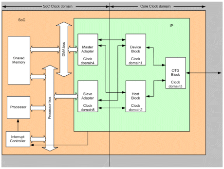
Figure 2. USB OTG IP architecture
The clock domains within the IP are divided into two regions.
- System level clock domains
- Core level clock domains
The interfaces towards the system bus are working on system bus clock domain and the IP core itself is working on a 48MHz independent clock domain. By separating this way, we got two advantages. The IP core functionality becomes more or less independent of system bus clock frequency (in our case we are able to work from a system bus clock ranging from 20 MHZ to 150 MHZ). With the above partitioning, it becomes easy to implement the power management scheme. This means power management is possible both from the IP core point of view, and from the SoC point of view and both are independent to each other. For example on the DMA path, if there is a data transfer to be accomplished on behalf of the IP, then the IP will request for the system bus clock to complete the data transfer. On the other hand if the processor is making an access to the IP registers, then the processor turns on the system bus clock. The core level power management is completely handled by the core itself.
The software interface for the IP is made based on command and status register (CSR) architecture. This is shown in the figure [3]. This way the effective load on the on the SoC processor ( MIPS requirements ) is reduced.
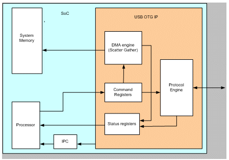
Figure 3 USB OTG IP Command and status register architecture
5.2. Design & development
The first activity carried out here was the separation of the functional requirements from the SoC specific requirements. The IP core is working a local core clock (independent of SoC bus clock) and this way all IP core specific logic made synchronous to the local clock. This made the design simple.
The second one is that the IP is designed according to the CoreUse (Philips internal methodology for design reuse) guidelines. This means standardized views were created for the IP.
The third and the most important aspect is on design reuse. Here we reused an existing USB device and host design databases. The following approach followed.
- Scheduled sufficient time to get familiar with the code
- Derived a golden configuration of the IP to work with
- Followed a wrapper approach in adding new functionalities
- Developed a completely automatic verification environment for the functional verification
By deriving a golden configuration, we got a much better control over the application space of the IP. This is done in consultation with the SoC community. By this way we made sure that most appropriate use cases for the IP are incorporated, and at the same time, verification scope for the IP become more focused.
By incorporating a wrapper approach, we made sure that the core IP logic is not touched. This again helped us in reducing the verification time. However this had some side effects like additional gate count & latencies.
5.3. Verification
Here the basic assumption made is that, there is no modification done to the core logic. Only additional functionalities are added through a wrapper approach.
Block level verification: For the new modules generated, we carried out block level verification. Hardware verification language based tools like Specman [8,9] is used here.
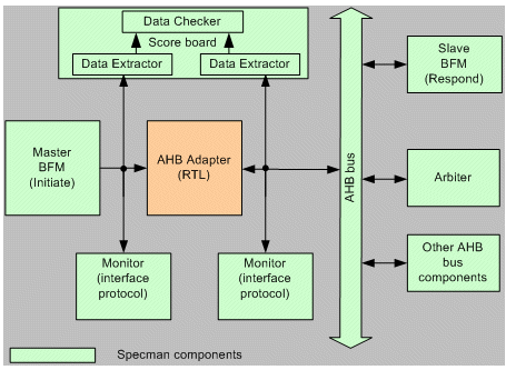
Figure 4 Block level test environment using Specman
The figure [4] represents the test environment used for testing the AHB system bus adapters.
Functional Verification: After the block level testing, the modules are integrated, and the following were the scope of testing here.
- Integration verification
- System level hardware functional verification
- Software interface verification
- Out of box testing
- Test environment for SoC integration
In order to accomplish the above, a generic ARM (ARM7TDMI) SoC simulation environment was created (figure [5]).
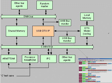
Figure 5 Integration test environment for USB OTG IP
The key characteristics of the above test environment are:
- Represents a typical SoC
- Supports ‘C’ bases test cases. So useful for software driver testing
- Interface monitors can provide debug information. For example the USB bus monitor was with GUI and designed based on industry standard CATC [7] format.
- Supports automated test cases.
The IP had two interfaces. The first one is the USB bus interface towards the external world. The second one is the AHB system bus interface towards the system bus. The AHB compliance verification was carried out by using a Specman AHB eVC [9].
The USB functionality is handled by a combination of hardware and software. Here it was not easy to carry out complete testing in a simulation environment. This was planned on a FPGA prototype environment, where in the USB core is working at the actual speed. The USB compliance verification was carried out as per the OTG compliance test plan [5].
Hardware Software co verification: This was also planned using the FPGA prototype based on ARM integrator board
The key characteristics are
- The USB IP core is running at the actual speed
- Can be used for testing against third party USB systems
- USB and OTG compliance testing can be performed
- Application level testing is possible
On the support and maintenance front the following are ensured as a part of delivery
- RTL is technology independent (valid only for RTL delivery).
- Synthesis scripts for technology mapping
- DFT flow is exercised on the netlist to ensure >98% coverage
- A stand alone test benches is provided with the delivery
- Documentation like data sheet user manual etc. are provided
Apart from this a dedicated delivery support and maintenance team is maintained, and the typical tasks carried out by this team includes the following.
1. On site integration support
2. Support for porting integration test cases
3. Resolving issues faced by the customer
4. Support for post silicon verification
5. Support for USB logo certification
6. Conclusions
The following lessons learned during the development of the USB OTG project.
- If the design complexity is high, then it makes sense to reuse existing IP blocks. However a process must be in place to address the following aspects
- To assess the state of the design database so that an estimate of the work involved in productizing the design can be prepared. The result of this examination should confirm whether it makes economic sense to use the existing database, or whether it is actually better to start again
- The verification environment available with the design database should be useful in the re-usable IP context also
- Today around 70 % of the total IP development effort is spend on verification of the IP. This means a methodology based on verification reuse must be in place so that the verification framework can be used across the development cycle and possibly for another project.
- Attention to be given in understanding the SoC level requirements so that a seamless integration of the IP is possible with the SoC. The following approach would be beneficial.
- Create a golden configuration for the IP by looking into the typical use cases. So only this configuration need to be verified, and this configuration can satisfy 90% of SoC community.
- It is preferable to have DMA capable IP with command and status architecture view for the software interface. This makes the IP integration smoother, because the SoC integrator does not have to worry much about the load on SoC CPU.
- The IP must have a completely automated test environment. The IP integrator must be able to reuse the verification environment in his SoC
- The test environment and cases must be easily portable to SoC. Here HDL test environment and ‘C’ level test cases are preferred with API standardization. In this way the test application running at the SOC can interact with the DUT through the standardized API’s
- A functional prototype is a must for HW/SW co-verification. Even though the prototype may not work at the actual working speed, the environment can provide a platform for the following
- HW/SW co-verification.
- Platform for software development.
- IP demonstration platform
- USB Specification, Rev 2.0 27th April, 2000
- On-The-Go supplement to the USB 2.0 Specification, Rev 1.0a 13th June, 2003
- AMBA Specification 2.0
- Open Host Controller Interface Specification for USB, Rev. 1.0a, 14th September, 1999
- On-The-Go Compliance Plan for the USB 2.0 Specification, Rev 0.69, 19th April, 2002
- CATC USB analyzer
- Specman Elite product brief -
Related Semiconductor IP
- SHA-256 Secure Hash Algorithm IP Core
- EdDSA Curve25519 signature generation engine
- DeWarp IP
- 6-bit, 12 GSPS Flash ADC - GlobalFoundries 22nm
- LunaNet AFS LDPC Encoder and Decoder IP Core
Related Articles
- Integrating VESA DSC and MIPI DSI in a System-on-Chip (SoC): Addressing Design Challenges and Leveraging Arasan IP Portfolio
- Reusable debug infrastructure in multi core SoC : Embedded WiFi case study
- Context Based Clock Gating Technique For Low Power Designs of IoT Applications - A DesignWare IP Case Study
- Formal Property Checking for IP - A Case Study
Latest Articles
- TensorPool: A 3D-Stacked 8.4TFLOPS/4.3W Many-Core Domain-Specific Processor for AI-Native Radio Access Networks
- Assertain: Automated Security Assertion Generation Using Large Language Models
- VolTune: A Fine-Grained Runtime Voltage Control Architecture for FPGA Systems
- A Lightweight High-Throughput Collective-Capable NoC for Large-Scale ML Accelerators
- Quantifying Uncertainty in FMEDA Safety Metrics: An Error Propagation Approach for Enhanced ASIC Verification