Real-Time Video System Design Based on the NIOS II Processor and µCLinux
Abstract:
In this paper, a modular, configurable and versatile hardware platform for real-time video and image processing is presented. The hardware platform is based on the Altera STRATIX development board which is completed with a Camera interface for video acquisition and a VGA interface for image restitution. The platform supports simultaneous HW/SW co-design and partitioning. The system main part is the Altera NIOS II soft core processor for data processing. During this study, we have used video sequences, which are acquired, processed and visualized while respecting temporal constraints. The whole of system was made under µClinux and was performed on the NIOSII soft core processor. Simulation and Synthesis results are presented and prove that our video system respect the real-time constraint.
1. Introduction
Over the last decade, the popularity of Field Programmable Devices to implement digital circuitry has seen a significant increase. The FPGA is the most spectacular programmable device and it has a several advantages, such as their fast manufacturing turnaround time, low start-up costs and conception easiness. With increasing device density, audacious challenges become feasible and the integration of embedded architectures is significantly improved [1] [2]. In video application, and especially in video processing, the impressive evolution of algorithms and the emergence of new techniques dramatically increase the complexity of algorithms. This computational aspect is crucial for many real-time applications and in the most cases, programmable devices become the best option [3] [4].
This paper is organised as follows: Section 2 gives a short description of the real-time video system. Section 3 describes the embedded video system, the camera and VGA hardware interfaces as well as the synchronization of these two interfaces and the temporal constraints to respect. The implementation of the whole system is presented in Section 4. Finally, a conclusion and future work are presented in Section 5.
2. Real-Time System-On-Chip
The goal of real-time systems especially hard real-time systems is often to guarantee that a response can be made to an input signal by a fixed deadline, even in the worst case situation. Worst case calculation times tend to be more important than average instruction execution rates. For complex real time systems with many tasks, many signals and many deadlines, a software solution to a real time multi-tasking environment leads to a very conservative computing solution. A powerful processor is needed to guarantee response ties even for very rare conjunctions of events.
Being able to respond to inputs with customised hardware modules has obvious advantages. Many parallel hardware units can all operate in parallel, so that individual response times are much less variable and easier to guarantee, even as number of tasks increases. Hardware units are not so affected by issues such as task swapping, scheduling, interrupt service, and critical sections, which complicate real time software solutions.
Our research goal is to clearly demonstrate and prove these advantages through the study and conception of video system.
2.1. Video System
In our video and image processing application, the chain contains modules of acquisition, processing and restitution of a video signal coming from the video source. Therefore, for us the real-time is the fact that the acquisition and the processing should not introduce delay which leads to the loss of useful data for the video restitution.
The global processing video system is based on a System On Programmable Chip (SOPC) by which all system components are put on a single chip (FPGA). The synoptic diagram of the realized system is presented in figure 1.

Figure 1. Synoptic of the video system
The FPGA is integrated into a modular architecture composed of three modules:
- Main Board: This is the core of the system. It was designed around a Stratix EP1S10 component manufactured by Altera. This component is optimized for the implementation of SOPC by integrating a NIOS soft core processor. A NIOS processor is a user configurable soft core processor. Several peripheral devices and connectors (UART, LCD, VGA, Ethernet etc) serve as interfaces between the Stratix FPGA (Field Programmable Gate Array) and the external environment [5]. 8 MByte FLASH, 16 MByte SRAM and 1 MByte SRAM allow implementation of the complex FPGA applications. For our video and image applications, we are using flash memory, SRAM, SDRAM, UART and timer.
- PULNIX Camera: The camera provides in its output 8-Bits video data, a pixel clock at 14.318 MHz frequency and synchronization signals: line synchronization (LDV: Line Data Valid) and frame synchronization (FDV: Frame Data Valid). The camera rate is 30 images/s.
- VGA Display: VGA monitor for the images restitution which have a 640x480 resolution in greyscale. The transmitted data stream towards the monitor is 25 Mo/s. The VGA monitor displays 60 images/s.
3. Adopted design
In this section, the FPGA adopted design is detailed. This design is composed by different dedicated IPs modules (Intellectual Property). Each module is dedicated to a specific function.
3.1. IPs Modules
IPs for programmable logic devices can be divided into three classes: soft, firm and hard core. A soft core is a synthesizable hardware description language of a functional component. The outstanding advantage of a soft core is the technology independence of the description and the flexibility to adapt it to any specific application requirement. However, the flexibility also leads to news challenges in reaching a given performance (timing or area). A firm core is a synthesized, pre-placed and routed HDL description. A firm core is less flexible and in most cases dependent on a specific FPGA technology. The fixed design topology leads to higher performance and more reliability in comparison to a soft core. Finally, a hard core is a fully designed, placed and routed ASIC layout. This type of IP is optimised for timing, power and area performance but only the FPGA manufacturer is able to integrate hard core into the PLD production process. As a consequence hard core is least flexible and heavily technology-dependent.
3.2. Embedded video system
Our embedded video system is composed of three IPs modules: a NIOS II soft core processor, camera interface hardware core and the VGA interface hardware core. The main processing core of the embedded video system illustrated in figure 2, is The Nios II CPU. It is connected to hardware peripherals via a custom Altera Avalon bus. The bus has a parametric master/slave type. The parameterized Avalon bus interfaces are automatically generated by a special Altera Nios generating tool (SOPC Builder) for every custom peripheral integrated into the design.
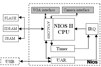
Figure 2. Block diagram of the implemented video system
The Altera NIOS II soft core processor (FAST version) is a 32-Bits scalar RISC with Harvard architecture, 6 stage pipeline, 1-way direct-mapped 16KB data cache, 1-way direct-mapped 16KB instruction cache and can execute up to 150 MIPS [6]. The main interest of this soft core processor is its extensibility and adaptability. Indeed, users can incorporate custom logic directly into the NIOS arithmetic logic unit (ALU) [7]. Furthermore, users can connect into the SOPC the on-chip processor and custom peripherals to a dedicated bus (Avalon Bus). Thus, users can define their instructions and processors peripherals to optimize the system for a specific application. Block diagram of the NIOS II soft core is illustrated in figure 3.
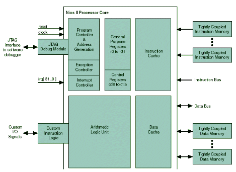
Figure 3. Architecture of the NIOS II soft core processor
From figure 2, we see that the camera and the VGA interfaces are connected to the NIOS II CPU, SRAM and others hardware peripherals through the Avalon Bus. The data transfer between the Camera interface, VGA interface and the SRAM can be realised by using the CPU. A C program allows to manage and to make this transfer. A temporal constraint is imposed by the fact that the Camera buffer must be empty in some clock cycles, to be aligned with the Camera stream and to present the data to the VGA interface with a fixed delay. The use of the CPU reduces the transfer speed because the interruption initialization and the instructions execution of the C program are slow. Indeed, the transfer of 32 Bits word through the CPU requires a ten clock cycles. For this, we must have 768000 clock cycles for one image transfer.
Our purpose is to have a maximum free time to satisfy the real-time constraints in video processing. To solve this problem, we chose a hardware solution which consists in the realization of a DMA (Direct Memory Access) component allowing the direct data transfer between Camera interface, VGA interface and SRAM. The DMA-Camera and DMA-VGA components are described in VHDL language. They allow to accelerate the data transfer between camera, SRAM and VGA interfaces.
In the next section, we describe the IP module for Camera and VGA interface and the synchronisation between them.
3.3. Interface
3.3.1. Camera interface
The general structure of the camera interface is presented by the following synoptic:
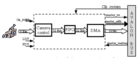
Figure 4. Synoptic of the camera interface
This interface consists of three modules. The camera control module allows to send the acquired video data towards the FIFO (First In First Out) module with 32-Bits words. Indeed, in the purpose of using the 32-Bits bus size totality, each four 8-Bits data pixels must be processed at 32-Bits word.
The FIFO allows to memorize image line (640 pixels). It is like a buffer between the data writing and reading. The writing on the FIFO is synchronized with the Camera clock. On the other hand, the reading is synchronized with the system clock (50 MHz). Indeed, it is necessary that the reading of the FIFO data towards the SRAM is quite fast to follow the Camera stream.
The third module is the DMA that allows the data transfer from the FIFO towards the SRAM through the Avalon bus by sending «master_w», «master_addrw» and «master_wrdata» signals. The writing cycle extends until the Avalon bus sends «master_waitreq» signal.
The camera interface permits us to send the acquired video data and other control signals towards the Avalon bus.
3.3.2. VGA interface
The general structure of VGA interface [8] is presented by the following figure:
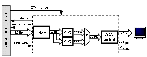
Figure 5. Synoptic of the VGA interface
This interface consists of three modules. The DMA module allows to transfer the data from the SRAM towards the FIFO by using «master_rd» (starting the reading of the master from the slave) and «master_addrw» (addresses sent towards the Avalon bus) signals.
A buffer module is composed of two FIFO which have the same depth (640 pixels for one image line). Indeed, if the DMA writes in the first FIFO, the VGA controller module reads from the second FIFO. This last module sends « R », « G », « B » and synchronization signals towards the VGA extension board (HS: Horizontal Synchronization signal and VS: Vertical Synchronization signal) [9].
The writing on the FIFO is synchronized with the system clock (50 MHz). On the other hand, the reading is synchronized with VGA clock (25 MHz). The achieved interface allows to transfer the 32-Bits data from the Avalon bus towards the visualization VGA monitor.
3.3.3. Synchronization between the Camera and VGA interface
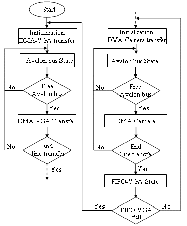
Figure 6. Interfaces synchronization
To permit the acquisition and the restitution of the image, the Camera and VGA interfaces must share the same SRAM slave. A problem may happen if the VGA and Camera interfaces access SRAM at the same time (Since the Avalon Bus sends the same «master_waitreq» signal to these two interfaces). To improve the functioning of the system, synchronization is necessary between these two interfaces which are presented by the flowchart in figure 6.
As shown in figure 6, an interface can begin the data transfer only if the other ends. In our case, the VGA interface has priority since a data transfer discontinuity between the SRAM and the FIFO-VGA causes problems while displaying video. For this, the DMA-Camera transfer starts only when the DMA-VGA transfer is finished.
This DMA-Camera allows the transfer of 32 Bits word in one clock cycle. For the image transfer, we need 76800 clock cycles. In this way, the DMA-Camera transfer is ten times faster than that of the CPU.
The stream of data coming from the camera is of 14 Mo/s. The useful video is composed by 640x480 pixels. Since the DMA-Camera transfer requires one clock cycle for each 32 Bits word, the total transfer time of an image is 1.536 ms. Therefore, the image transfer represents 4.7% of its duration by using the system clock (50 MHz) with 30 images/s camera rate. The transmitted data stream towards the monitor is 25 Mo/s. The total transfer time of one image by DMA-VGA is 1.536 ms.
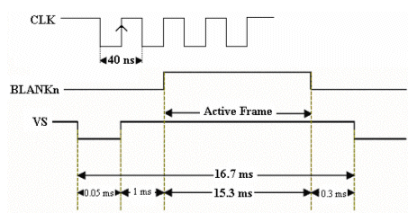
Figure 7. Vertical Video Timing (Frame)
The previous chronogram represents the needed time to display one image by VGA monitor which is equal to 16.7 ms [9]. The DMA-Camera transfer of one image requires 1.536 ms which represents 9.2% of the total time, in the same way for the DMA-VGA transfer. Thus, 18.4% of the image period would be necessary for the Camera and VGA transfer and 81.6% remain free for the real time processing.
4. FPGA implementation of the video system
4.1. Implementation on FPGA
Every hardware core is described in VHDL. We have used the ModelsimTM simulator from Model Technology and the Altera Quartus tools for circuit synthesis and target implementation. When the hardware is designed, there are two options how to port software applications on the board. The first is to use Linux operating system. On the NIOS II soft core processor and various peripheral hardware cores (Ethernet, UART, VGA, etc.), we can port derivative of Linux kernel (µClinux) which is intended for microcontrollers without Memory Management Units (MMUs) [10]. The port of µClinux on the NIOS II core is licensed under the terms of the GNU General Public Licence (GPL) [11]. The second option is to use the monitor program which is loaded into the RAM of the NIOS II controller. This method is used during the development cycle. When the application meets the requirements, it is compiled for the Linux operating system.
4.2. Implementation results
Table 1 shows implementation results of our video system in the Altera Stratix EP1S10 FPGA which is based on 1.5V, 0.13µm technology with a density that reaches 10570 Logic Elements (LEs), 113KB of Embedded System Blocs (ESBs), 48 DSP blocks and 427 Input/Output Blocks (IOBs) [12][13][14]. Results in the Table 1 have been obtained with separate implementation of the particular modules (NIOS II soft core processor, camera interface and VGA interface).
Table1. Table of the results
| Number of | NIOS II (FAST) | Camera Interface | VGA Interface |
| LEs | 40% | 5% | 7% |
| ESBs | 36% | 1% | 1% |
| DSPs | 16% | 0 | 0 |
| IOBs | 31% | 34% | 40% |
The complete implementation of our system video utilizes 57% of the LEs, 40% of the ESBs, 16% of the DSP block and 41% IOBs. The maximum frequency is 68.6 MHz. This frequency is limited by the memory access time and delay caused by connection with all other peripherals. The implementation of our embedded video system on the FPGA allows us to obtain an SOPC.
The implementation of the various peripherals constituting our system leaves sufficient space on the STRATIX programmable component for the addition of other IPs modules and the integration of real-time video processing.
5. Conclusions
Based on configurable technology (FPGA, NIOSII soft core processor), a powerful prototype platform for image and video processing was designed in order to support HW/SW codesign and partitioning. The IPs modules for video acquisition and restitution are developed and based on DMA module in order to interface the two external modules with the FPGA component of the development board.
The system implementation on the programmable component uses 48% of the IOBs, 57% of the LEs , 40% of the ESBs and 16% of the DSP blocks.
The system frequency is 50 MHz. With this frequency, 18.4% of the image period would be necessary for Camera and VGA transfer and 81.6% for the real-time processing algorithms.
Our future project will consist to the integration of video processing algorithm by using our development board for real-time video applications.
6. References
[1] A.Dandalis and V.K.Prasanna, “Configuration Compression for FPGA-based Embedded Systems_ FPGA,” 2001, February 11-13, 2001, Monterey, CA, USA.
[2] P.Lysaght, “FPGAs as Meta-Platforms for Embedded systems,” IEEE International Conference on Field Programmable Technology (FPT’02),Hong Kong,2002.
[3] F. Ghozzi, P. Nouel, Ph. Marchegay, “Acquisition et mémorisation vidéo sur système Excalibur,” IEEE Canada, Conférence Canadienne en Génie Électrique et Informatique 2003, Montréal, Mai 2003.
[4] M. Finc, A. Trost, B. Zajc, A. Zemva, “ HW/SW Co-design of Real-time Video Applications Using a Custom Configurable Prototyping Platform,” Electrotechnical Review, Ljubljana, Slovenija, May 21, 2003.
[5] Carte de développement: ALTERA NIOS STRATIX http://www.rennes.supelec.fr/ren/fi/elec/fpga/altera/nios stratix/nios_stratix.htm.
[6] Nios documentation http://www.altera.com/literature/lit-nio2.jsp
[7] J. Cong, Y. Fan, G. Han, A. Jagannathan, G. Reinman, Z. Zhang, “Instruction Set Extension with Shadow Registers for Configurable Processors,” FPGA’05, February 20–22, 2005, Monterey, California, USA.
[8] Lancelot Home Page, “VGA video controller”, http://www.fpga.nl.
[9] M. Groeneveld “VGA video controller for the Altera Excalibur processors” Data Sheet, version 2.1, May 1st, 2003.
[10] The µClinux project http://www.uClinux.org.
[11] The NIOS Forum http://www.niosforum.com/forum.
[12] D.Lewis and Al, “The StratixTM Routing and Logic Architecture,” FPGA’03, February 23-25, 2003, Monterey, California, USA.
[13] Altera Data Sheet, “Stratix Device Family,” version 3.1, September 2004.
[14] High-Performance Stratix Architecture «http://www.altera.com/products/devices/stratix/ features/stx-architecture.html ».
About the Authors
(1) Laboratory of Electronics and Information Technology
National Engineers School of Sfax (E.N.I.S.), BP W 3038 SFAX - TUNISIA
Nouri.Masmoudi@enis.rnu.tn
(2) IXL laboratory –ENSEIRB - University Bordeaux1 - CNRS UMR 5818,
351 Cours de la Libération, 33 405 Talence Cedex, France
{benatita;kadionik;nouel;marchegay}@enseirb.fr
Related Semiconductor IP
- NPU IP Core for Mobile
- MSP7-32 MACsec IP core for FPGA or ASIC
- UHF RFID tag IP with 3.6kBit EEPROM and -18dBm sensitivity
- NPU IP Core for Edge
- Specialized Video Processing NPU IP
Related White Papers
- AI, and the Real Capacity Crisis in Chip Design
- A Survey on the Design, Detection, and Prevention of Pre-Silicon Hardware Trojans
- VLSI Based On Two-Dimensional Reconfigurable Array Of Processor Elements And Theirs Implementation For Numerical Algorithms In Real-Time Systems
- Using HW emulators to get HW/SW right the first time on the Sun UltraSPARC T1 processor
Latest White Papers
- Ramping Up Open-Source RISC-V Cores: Assessing the Energy Efficiency of Superscalar, Out-of-Order Execution
- Transition Fixes in 3nm Multi-Voltage SoC Design
- CXL Topology-Aware and Expander-Driven Prefetching: Unlocking SSD Performance
- Breaking the Memory Bandwidth Boundary. GDDR7 IP Design Challenges & Solutions
- Automating NoC Design to Tackle Rising SoC Complexity