NVM on Advanced Nodes for Smartphone & HPC Platforms
By eMemory
In the applications of high-performance computing and high-end smartphones, chip designers are chasing high-profit margins, and customers are looking for products with the best performance and security. These demands create a powerful driving force, pushing foundries to keep up with Moore’s Law and IP vendors to keep providing high-performance IPs. Among the IP demands, the embedded nonvolatile memory family is one of the key fundamental IPs in the advanced nodes.
With EUV photolithography technology’s maturity, TSMC is adopting more EUV steps on the N7 platform and rolling out more cost-effective and higher transistor density N6 solutions for mainstream products, including smartphones and consumer electronics, base station, networking communication, AI, and autonomous applications. eMemory, the leading and reliable, pure eNVM IP provider, works closely with world foundries and provides the best high reliable/secure NeoFuse/NeoPUF IPs on the most advanced and up to date FinFET processes for trimming, function selection, key storage, and inborn secure key functions.

Because of the extremely high price of product development and reticles in advanced nodes, fabless design houses tend to include multiple functions into one single SoC to lower the average cost. These multi-function chips are divided into different market segments or grades via function setting flow at the wafer sorting stage or after packaging. A truly reliable and easy-to-use embedded OTP plays a crucial role in realizing the function selection features. Other scenarios like chiplets used in data centers, the interface and communication protocols revised regularly, and the system operators are forced to keep upgrading the firmware and hardware settings. Therefore, adopting embedded OTP in the chiplet in chip architecture design is the most cost-effective way to minimize the chip replacement cost and increase the maintenance efficiency
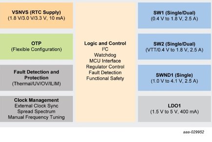
Compared to 4G smartphones, the power demands in 5G are getting much higher along with the exponential growth of data communication, processing, and reaction. An embedded or discrete, multifunctional, and smart power management function, can provide a precise regulated voltage source to increase system performance and lower down the overall power consumption. A high-quality embedded OTP is always equipped with these kinds of chips to execute analog trimming duties.

Besides the fundamental function selection and trimming purposes, data and entity security is gaining attention in automotive, cell phones, communication, and consumer chips in the modern digital world. A secure and certified embedded OTP can store UID, HUK, public keys, and private keys to realizing entity identification, authentication, anti-counterfeiting, data protection, and secure boot functions to construct a “security everywhere” digital world.
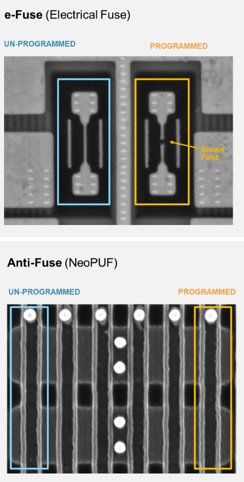
In some foundries, a poly or metal eFuse-type OTP is provided as a standard module. Although it is easy to design and use, this technology suffers serious electron migration and faces limitation issues on reading times. Besides, the blowout of poly and metal lines is easily indicated through an optical microscope. As a result, eFuse OTP cannot provide the necessary reliability and security levels to fulfill market requirements in advanced nodes.
eMemory’s innovative quantum tunneling NeoFuse OTP is extremely secure with inherent invisible properties. NeoFuse’s advantages include a stable quantum tunneling path to support automotive grade 0 excellent reliability performance. It also has a small footprint with a core device-based cell structure and a flexible control interface. When chip makers consider a suitable OTP solution for their SoCs in advance nodes, NeoFuse is undoubtedly the best choice.

In 2016, NeoPUF, a security solution based on the NeoFuse technology was invented and received the ISSCC 2018 Outstanding Far-East Paper award. Physically Unclonable Function (PUF) is an inborn random bitstream produced along with the uncontrollable variations in manufacturing flows. With proper PUF technology, people can remove the UID/HUK program procedures, effectively reduce the attack surface, and use it as a reliable “root of trust.”
Since the quantum tunneling PUF originates from NeoFuse technology, it shares the same fundamental cell design and operating schemes, meaning NeoPUF has the high reliability and security performance that NeoFuse does. Another advantage is NeoFuse and NeoPUF can be combined easily in one single hard IP to provide both inborn random bitstreams from NeoPUF and be programmed with important data in the NeoFuse area.
NeoPUF is a true ideal PUF and improves reliability and randomness compared to the traditional SRAM PUF. Because of the excellent retention and randomness performance, ECC, error correction code, and HASH is not necessary. It can be considered the most important and reliable “root of trust” and execute true secure boot procedure with instant ready features.

NeoFuse and NeoPUF are now available on the N6 platform providing customers with additional cost-effective benefits for a broad array of applications ranging from high-to-mid end mobile, consumer, AI, networking, 5G infrastructure, GPU, and high-performance computing. Furthermore, NeoFuse and NeoPUF are under development on the N5 platform which will be ready by Q2/2022.
Related Semiconductor IP
- ReRAM NVM in SkyWater 130nm
- Memory (SRAM, DDR, NVM) encryption solution
- Universal NVM Express Controller (UNEX)
- NVM Express (NVMe) Controller (compliant with NVMe 1.4 Base Specification)
- NVM OTP in Huali (40nm, 28nm)
Related White Papers
- Scalable Architectures for Analog IP on Advanced Process Nodes
- Interstellar: Fully Partitioned and Efficient Security Monitoring Hardware Near a Processor Core for Protecting Systems against Attacks on Privileged Software
- One Platform, Five Libraries: Certus Semiconductor’s I/O IP Portfolio for Every Application on TSMC 22nm ULL/ULP Technologies
- Memory Prefetching Evaluation of Scientific Applications on a Modern HPC Arm-Based Processor
Latest White Papers
- Ramping Up Open-Source RISC-V Cores: Assessing the Energy Efficiency of Superscalar, Out-of-Order Execution
- Transition Fixes in 3nm Multi-Voltage SoC Design
- CXL Topology-Aware and Expander-Driven Prefetching: Unlocking SSD Performance
- Breaking the Memory Bandwidth Boundary. GDDR7 IP Design Challenges & Solutions
- Automating NoC Design to Tackle Rising SoC Complexity
