NetComposer-II: High performance Structured ASIC Programmable NPU platform for layer 4-7 applications
Hsinchu, Taiwan
Abstract
:
This paper presents Faraday Technology's structured ASIC platform solution for developing networking system-on-chips which have gigabit-per-second layer 4-7 throughput.
The platform architecture is briefly introduced, and the IP blocks (including the CPU complex, structured ASIC blocks, and programmable SerDes interfaces) are detailed. Finally, typical target applications and implementation are presented for reference.
INTRODUCTION
As Ethernet becomes the pervasive protocol to deliver networked data, there is an increasing need to apply intelligence to traffic flow (e.g., content networking and security), and translation between legacy interfaces and Ethernet. In both cases, there is a growing demand for systems to take Gigabit and 10-Gigabit Ethernet traffic and perform deep packet inspection before forwarding the data.
Ever since the late 1990's, semiconductor companies have attempted but failed to develop network processors (NPUs) to improve the performance of looking very deep into the packets – the so-called layer 4-7 algorithms. Most of these chips have been too complex, too limited, too expensive, or too slow to meet customers' needs. What customers would like is chips which contain all of the standard components needed, and yet still have enough ASIC programmability at very low cost. To satisfy network system developers' needs, Faraday has developed the NetComposer product family, the industry's highest performance NPU with structured ASIC programmability for layer 4-7 processing, yet the end products cost only $50.
This paper describes the architecture of Faraday's NetComposer-II (NC-II). This structured ASIC platform has been designed to combine the silicon-proven assurance of an application specific standard product (ASSP) with the proprietary advantages of a custom ASIC. Most of the IP blocks have been pre-defined, pre-verified, and pre-manufactured to accelerate time-to-market and to split the mask charges among several ASIC projects, while users can use the metal-programmable cell array (MPCA) structured ASIC blocks and the final five mask layers to integrate their own designs.
The first section of this paper will give a brief product overview to the NetComposer platform architecture. The following section details the most important IP blocks in this platform, including the CPU complex, the structured ASIC blocks, and the programmable SerDes interfaces. Finally, this paper exposes several target applications for the NC-II platform.
PRODUCT OVERVIEW
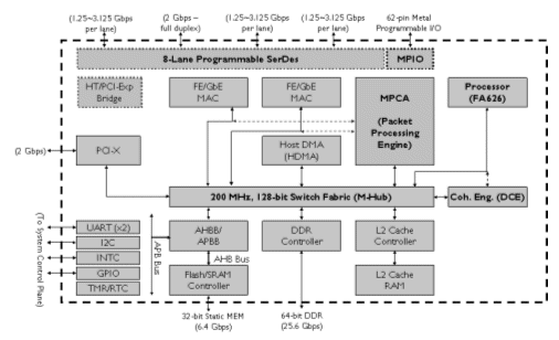
The NetComposer-II (NC-II) is a combination of a full-featured NPU ASSP with the programmability of Faraday's structured ASIC technology. It combines software programmability of a high performance CPU with three-million gates of structured ASIC logic and eight programmable SerDes lanes to deliver the maximum flexibility in performance and application. The most important blocks are shown in Figure 1.

Figure 1: Block Diagram of the NC-II
CPU Complex:
At the heart of the NC-II is a proprietary ARMv4 CPU developed by Faraday, code-named FA626. It consists of a CPU core, a branch target buffer (BTB), I/D-cache, I/D-scratchpad, a memory management unit (MMU), a write buffer, data coherence and bus interfaces. With the 8-stage deep pipeline microarchitecture, the FA626 processor core delivers high speed operation frequency of 600MHz in 0.13um logic process.
The I-/D- cache make use of program and data locality to improve processor performance. The FA626 features a 32KB, least recently used (LRU), 4-way set-associated I/D cache.
The NC-II memory subsystem uses a core centric system interconnection to achieve variety of packet processing requests, such as high bandwidth demand, minimum latency requirement, and high packet throughput. The central controller, M-HUB, is a 8-to-2 switch fabric with a 128-bit, 200MHz, PVCI interface to manage and schedule multi-thread burst accesses to the on chip L2 cache and external DDR DRAM. The memory bandwidth is divided into 16 memory access time slots. For each time slot, the M-HUB provides the programmability to system designers to fine-tune the traffic for bandwidth and latency. The memory utilization can be enhanced by 40% through the time slot partition, programmability and arbitration.
In addition to the M-Hub, the L2 cache and the DDR controller, the memory subsystem also incorporates a centralized data coherence engine to ensure the data consistency among the system memory and processor’s local memory. Most of the data coherence checking and management are done by the Data Coherence Engine (DCE) to simplify the CPU’s design, so the CPU just accepts command from the DCE and gives the L1 notification feedback.
For the NC-II, there is a smart DMA engine which supports a rich set of features such as "scatter-gather" and "descriptor chaining". Through these features, the DMA engine significantly offloads the processor from frequent interrupts and context switching.
Structured ASIC:
Network system designs have a wide variety of market requirements on performance, flexibility, cost, time-to-market, product roadmap, features, etc. System designers make the best optimized design through different architecture evaluation. Table 1 shows a brief comparison among those architectures.
Table 1: Packet processing implementation comparison
| (all chips in 0.13um) | ASSP NPU | CPU + ASIC | NC-II CPU + MPCA |
| Manufacturing Time | 0 | 120 Days | 30 Days |
| NRE Cost | 0 | > $1M | $300K |
| Performance | Good | Best | Best |
| Chip Cost | Best | Poor | Best |
| Differentiation | None | Best | Good |
The table shows that an ASSP NPU is good for time-to-market, cost and performance, but it could not have product differentiation and flexibility for features enhancement. One of the most powerful features of the NC-II, and what also differentiates it from all the other NPUs, is its structured ASIC capability. By using Faraday's patented Metal Programmable Cell Array (MPCA) structured ASIC, a designer has 3 million ASIC gates and 1.5 million bits of SRAM to incorporate proprietary algorithms into their own design, thus greatly accelerats the packet processing.
The structured ASIC approach is very similar to developing custom ASICs, except at a much lower upfront cost, and just 30 days manufacturing turnaround time, instead of over 100 days for a traditional 0.13um ASIC process. With the structured ASIC technology, users can easily create a custom NPU for its unique approaches to high performance and intelligent packet processing capability.
Programmable SerDes:
As the high-speed line rate growing from current 10Gb to future 40Gb, system designers are facing the challenge to achieve high packet throughput under the concurrent request for L4~L7 intelligent packet processing at wire speed. Furthermore, for applications that require extensive processing of data, a single processor often provides inadequate performance. Serial and parallel architectures are the main options for multiprocessor design. So except the high-speed packet processing, the chip-to-chip interconnect also significantly influences the system performance.
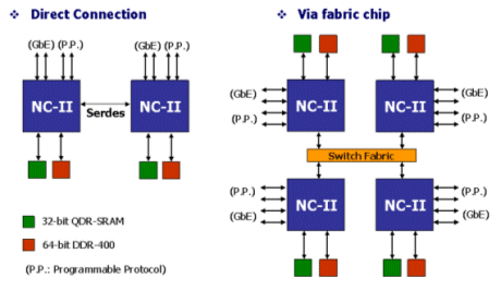
Figure 2 shows the system performance enhancement can easily be implemented by multiple NC-II chips extension through their SerDes interfaces. The inter-chip interconnection can be accomplished in either parallel or serial style, with or without Switch Fabric chips.

Figure 2: Muitiple NC-II Design
The NC-II breakthrough comes from its use of programmable SerDes. The NC-II incorporate a total of eight SerDes ports and the ease of programmability enables designers to configure these ports to any combination of several different protocols, including GigE, XAUI, Serial RapidIO, PCI-Express, HyperTransport, etc. By using the MPCA programmable logic, designer can implement the appropriate controller functions for these specified physical interfaces.
For storage systems, the parallel bus interfaces such as SCSI and ATA have been in the mainstream storage interconnect for over 20 years. With increasing bandwidth and flexibility demands, serial interfaces such as Serial ATA and Serial Attached SCSI gradually enter the mainstream. Serial ATA extends the ATA technology road map, delivering storage device interconnect speeds starting at 1.5G bps and up to 3G bps. SAS, comparing to the parallel SCSI interface, drives reliable point-to-point serial connections at speeds of up to 3G bps. The SAS interface is compatible with lower cost S-ATA, which offers a new level of price and performance flexibility to end users. System designer can easily achieve the optimized cost and performance design more efficiently and easily, by simply re-programming the SerDes and the controller logic for different standard with 3 top metal layer changes.
The NC-II SerDes is the industry's smallest and lowest power-consumption SerDes -- the per channel active power is only 80mw at 3.125Gbs, and per channel die size is 0.132mm2 for 0.13um process, which acted on the premise of fitting in the high speed serial interface specification, like XAUI, SPI4.2, and Hypertransport.
TYPICAL TARGET APPLICATIONS
Due to its high flexibility and programmable SerDes capability, the NC-II can be used in a wide variety of networking applications, including medium-to-large enterprise networks and carrier class networks.
In enterprise solutions, it can be used in gateway routers and switches, server load balancers, web-switches and LAN backbone switches. Similarly, in wide/metro/wireless area market segments, the NC-II can be used in edge service routers, wireless base stations and DSLAM for aggregating traffic or providing MSSP with high intelligence.
The NC-II also has the capability to address most of the transition of emerging and evolving protocol standards, including PCI-Express, Serial ATA, Serial RapidIO, and HyperTransport required by typical gateway routers.
Users can develop several generations of derivative chips to embrace all these interface changes. The following is an example to describe how use the NC-II for the system design of L4~ L7 packet processing.
L4~ L7 intelligent packet processing
There are many different services, like security, caching, load balancing, traffic statistic, billing and accounting, quality of service and admission control, that request network equipment to have the L4~L7 packet processing capability. System designers need to solve the challenge that performance must be fast enough for wide-speed traffic processing, flexible enough to support various service and future protocol and feature upgrade, and reliable enough to guarantee the service quality.
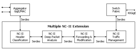
The major packet processing functions, include classification, deep packet analysis, forwarding & modification, and policing/statistic and traffic management. The distributed processing architecture can be implemented by simply serial cascading multiple NC-II chips. The architecture diagram is shown in Figure 3.

Figure 3: Distributed architecture diagram about L4~7 application implementation
The first NC-II executes header classification, which extracts bits from a packet header to form keys for routing table lookup operations. The search H/W accelerator can be implemented on the MPCA blocks to enhance the processing performance.
Once a packet has been classified, the second NC-II performs deep packet analysis. One best example is about HTTP protocol frame analysis. An http header indicates a web-based applications which can be deeply inspected into a wide variety of applications, including casual web-browsing, access to ERP, client/sever application, e-commerce transactions.
Another application about deep packet inspection or content filter protection, the NC-II embedded MPCA also can be use for H/W accelerator implementation.
After the packet had been classified and the lookup operations had been completed, the third NC-II forward the packet to destination directly or make any necessary modifications before the packet forwarding, e.g., by adding a tag for the traffic manager or switch fabric.
The last NC-II may need to police the packets against service-level agreements (SLAs), and may also collect detailed usage statistics on a per-flow basis for use in billing. Next, NC-II may do the scheduling and queuing of packets according to priority and network loading.
As the figure show, NC-II embedded re-programmable, high performance SerDes is competence to bridge and keep the wire speed data flow from line interface through inter-chip connection to switch fabric I/F to easily accomplish the 10G system performance.
Related Semiconductor IP
- NPU IP Core for Mobile
- NPU IP Core for Edge
- Specialized Video Processing NPU IP
- HYPERBUS™ Memory Controller
- AV1 Video Encoder IP
Related White Papers
- The Platform Based SOC Design that Utilizes Structured ASIC Technology
- A Flexible, Low Power, High Performance DSP IP Core for Programmable Systems-on-Chip
- Mixed Signal Drivers for Ultra Low Power and Very High Power Applications
- Optimizing High Performance CPUs, GPUs and DSPs? Use logic and memory IP - Part II
Latest White Papers
- Ramping Up Open-Source RISC-V Cores: Assessing the Energy Efficiency of Superscalar, Out-of-Order Execution
- Transition Fixes in 3nm Multi-Voltage SoC Design
- CXL Topology-Aware and Expander-Driven Prefetching: Unlocking SSD Performance
- Breaking the Memory Bandwidth Boundary. GDDR7 IP Design Challenges & Solutions
- Automating NoC Design to Tackle Rising SoC Complexity