The Platform Based SOC Design that Utilizes Structured ASIC Technology
by Yu-Wen Tsai and Shun-Fu Chuang
Faraday Technology Corporation
10-2, Li-Hsin 1st Road, SBIP
Hsin-Chu, 300, Taiwan
886-3-5787888-8729, 8004
Abstract
In this paper, we will introduce Faraday platform based SOC solutions that adopt Structured ASIC technology. The unique structured ASIC technologies developed by Faraday include Metal Programmable Cell Array (MPCA) and Metal Programmable I/O (MPIO). With these two metal programmable technologies, we can provide the most competitive cell structures, highest performance, and highest density with low power consumption. Base on our structured ASIC technologies, we proposed two complex platform based SOC design solutions TEMPLATE, and COMPOSER. The TEMPLATE is an FPGA-alike platform for general applications, and COMPOSER is the application-specific platform. Therefore, we can offer our customers an effective development environment to build their platform based SOC designs at a lower non-recurring engineering cost and a much shorter time-to-market.
1. Introduction
As shrinking process technology migration to very deep submicron, increasing chip complexity, more complicated verification tasks, but shorter time-to-market has multiplied the difficulty of designing systems-on-a-chip (SOC) in the deep submicron era. Moreover, the non-recurring engineering (NRE) cost, including implementation engineering effort and mask tooling charges, increases significantly as the process technology migration. The NRE cost is too expensive for all but the very high volume applications (quarter million plus units per year). And time-to-market pressure, frequent feature changes and product derivatives further exacerbate the cost issues. A new breed of ASIC products, called “Structured ASIC”, can cut NRE expenses by more than 90% for derivative chips, and speedup the time-to-market. As a result, the structured ASIC is becoming imperative for deep submicron designs. TABLE 1 is a cost comparison between typical 1-million-gate design 0.13mm process for FPGA, Structured ASIC and cell-based ASIC implementations.
We have proposed two structured ASIC technologies MPCA and MPIO as a low NRE cost with performance closer to cell-based solutions. With our structured ASIC technologies, the proposed structured ASIC implementation flow is exactly the same as the conventional cell-based ASIC flow because of Faraday competitive structured ASIC architectures. Moreover, Faraday has provided the structured ASIC logical synthesis, simulation, DFT synthesis, physical synthesis libraries compatible with existing commercial cell-based EDA tools.
Based on our structured ASIC technologies, we have proposed two platform based SOC solutions: TEMPLATE and COMPOSER. The TEMPLATE is an FPGA-alike SOC, which consists of the functional IPs, such as PLL, DLL, high-speed CPU, embedded RAM, and MPCA logics and MPIO pads, which can be customized for each application derivative. The COMPOSER solution is for application specific platform SOC. With the flexibility of structured ASIC technologies, TEMPLATE and COMPOSER can be reconfigured to implement the complex SOC designs.
Table 1: ASIC development cost
Source: Semiview December 2003
The rest of the paper will be organized as follows. Section 2 describes our structured ASIC technology. Section 3 shows the proposed platform-based SOC solutions TEMPLATE and COMPOSER. The concluding remarks follow in Section 4.
2. Faraday Structured ASIC Technologies
Faraday has provided two fundamental structured ASIC technologies MPCA and MPIO. The MPCA technology combines the advantages of cell-based library, including high density, high performance and low-power consumption, with the benefits of reduced NRE cost. The MPIO technology is used in reconfiguring I/O pads by one-metal-mask changing.
The MPCA technology is optimized for deep sub-micron designs with a focus optimizing routability, speed and minimizing power consumption. The MPCA is implemented as an embedded core cell array designed for functional changes through few metals and via layers. The MPCA technology allows customers to order wafers with about 90% of the layers already formed, then stock them up until future changes or corrections. This procedure can save a significant amount of NRE and turn-around-time from complex SOC. As shown in FIGURE 1, only the three metal layers are needed to program the library cells as well as place and route the design.
Figure 1: Programming layers for 7 metals process in mpca technology

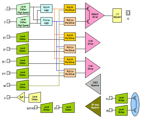
By changing just one top metal mask, MPIO technology can support PCI33, PCI66, PCIX, SSTL2 class I/II, CMOS, and TTL I/O with different drive strengths and slew rate controls. FIGURE 2 is a block diagram of Faraday’s MPIO.
With the leading structured technology, the implementation flow can be realized with the conventional EDA tool [1].
3. Platform Based SOC Design Solutions
With our MPCA and MPIO technologies, we offer two solutions to help designers to implement the complex platform based SOC designs in the 0.13mm and 90nm process era. These two solutions are (1) TEMPLATE and (2) COMPOSER. We would describe these two solutions in detail in the following sections.
Figure 2: Block diagram of metal-programming I/O (MPIO)
3.1 TEMPLATE
The complex platform SOC design usually contains timing and performance critical processors, embedded SRAM and analog peripherals IPs. The TEMPLATE ASIC contains high performance, and silicon-proven IP blocks such as DLL, PLL, embedded SRAM, 32-bit CPU and other embedded IP. Since there are few mask that need to be reconfigured for new applications, the manufacturing cycle for a complex SOC design is significantly shorter than the cycle required for a traditional cell-based ASIC. FIGURE 3 describes the floorplan overview of TEMPLATE ASIC. In order to maintain enough flexibility, to support a majority of customers, we have designed a family of TEMPLATE ASIC. TABLE 2 shows detail configurations of TEMPLATE family ASIC. With a wide variety of TEMPLATE configurations, customers can select the appropriate configurations for their specific applications.
Since the wide diversity of TEMPLATE ASIC configurations, it is very tedious for designer to initialize the design implementation. We have proposed a solution design kit Producer to ease TEMPLATE ASIC implementations. According to the inputs, Producer can help designers to select the appropriate TEMPLATE configuration as well as streamline the implementation process. If the required TEMPLATE configuration does not exists, we can work with designers to generate a customer own TEMPLATE configuration.
Figure 3: The floorplan overivew of template ASIC

Table 2: Template Family
*: Depends on different family configuration
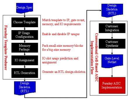
The proposed Producer implementation methodology is shown in FIGURE 4. Staring with inputs and Producer’s aiding, users can generate a design skeleton in RTL, and then follow the conventional cell-based ASIC implementation flow from logical synthesis to final physical implementation. The conventional cell-based ASIC flow has been developed for 10 years. The flow is very mature and robust, even in the very deep submicron design era. Based on the proposed methodology, we can take both the advantages of the flexibility in structured ASIC technology and the robustness in cell-based ASIC implementation flow.
The major functions of Producer are listed as follows:
3.1.1 TEMPLATE selection aiding
Producer can provide the TEMPLATE configuration briefing. Moreover, based on the inputs, such as number of I/O requirements, logic array size, Producer can select the best fitting configuration from the available TEMPLATE family.
3.1.2 Enable/disable embedded IP usage configuration
Each TEMPLATE configuration may contain several functional IP. Some of the functional IPs would not be used. The unused IP would be disabled in the final generated design skeleton RTL, and the input pins of a disabled IP will be tied to ground.
Figure 4: Proposed implementation methodology for template ASIC
3.1.3 SRAM packing
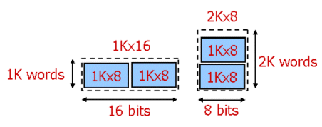
In additional to functional IPs, TEMPLATE ASIC also provide large amount SRAM blocks with different types memory architecture and different size, including single port and dual port SRAM ranging from 1K x 8 to 1K x 32. Unlike other structured ASIC vendor [2] solutions, TEMPLATE SRAM only can be implemented by using block SRAM blocks, not by programmable MPCA cells. By tiling and combining the embedded SRAM blocks, Producer can pack memory space that meet user’s need, and generate the companion SRAM packing netlist in Verilog RTL automatically. For example as shown in FIGURE 5, two 1K x 8 memory blocks can be packed a single 1K x 16 or 2K x 8 one. The automatic packing function has considered the physical locations.
Figure 5: Two 1Kx8 memory blocks can be packed into 1Kx16 or 2Kx8 memory
3.1.4 MPIO I/O assignment
The TEMPLATE family provides a wide range function of MPIO I/O that can be configured by one-metal interconnection changing. Producer can help I/O cells assignment by quick Drag & Drop to change the pin name, MPIO type and location.
3.1.5 Design skeleton generation in Verilog
Producer can generate a design skeleton according to selected TEMPLATE configuration. Users can plug their own design into the skeleton, and then passes the design to further logical synthesis and physical implementation.
3.1.6 Physical floorplan information generation
After the design skeleton generation, Producer has to generate the physical floorplan information based on the selected TEMPLATE configuration. The floorplan would guide the further physical implementation tasks.
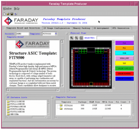
FIGURE 6 shows the Graphical User Interface (GUI) of TEMPLATE Producer. The GUI of Producer can provide the TEMPLATE briefing, embedded IP briefing, physical floorplan view, physical I/O assignment view, and visualized embedded IP setting. It is very useful for designer in reconfiguring the selected TEMPLATE ASIC in the early design stage.
Figure 6: Template producer
3.2 COMPOSER
COMPOSER, an structured ASIC technology based platform typically includes embedded processors, embedded RAM, external memory interface, analog IPs, or other peripherals such as interrupt controllers and DMA blocks. Besides the silicon-proven IPs, the remaining area of the COMPOSER chip is reserved for MPCA cells which can be easily programmed in the feature, with just three metal layer changes.
3.2.1 Faraday application specific platform
Faraday pushes a series of Application Specific Platform Solutions such as DisplayComposer for TFT/LCD display controllers, NetComposer for networking applications, MediaComposer for multimedia applications and IAComposer for information appliance applications.
FIGURE 7 shows the block diagram of IAComposer. The customers can implement their own functions by MPCA cells, and integrate with existing IPs by standard AHB bus interface.
Figure 7: The Block Diagram of IAComposer

FIGURE 8 shows the block diagram of DisplayComposer. The DisplayComposer consists of conventional standard cell block, embedded SRAMs, analog IPs, such as LVDS, and a configurable MPCA block. The MPCA block is configured as the timing control for TFT/LCD panel, because the timing control functions needs constant revisions due to different panel manufacture. FIGURE 9 shows the layout views of the DisplayComposer and NetComposer, respectively.
Figure 8: The block diagram of DisplayComposer

3.2.2 Customer own application specific platform
Additionally, customers are able to create their own exclusive platforms according to application-specific requirements. FIGURE 10 shows the layout view of the storage platform, which is co-developed by Faraday and a customer, where MPCA logics can be reconfigured to meet different FLASH memory specifications. This platform can be re-used for the various generations of products.
Figure 9: The layout views of DisplayComposer and NetComposer

Figure 10 The layout views of customer own storage platform
4. Conclusion
The structured ASIC technology is being used as a new approach to ASIC designs, which can cut down NRE cost, and also offer an impressive reduction in time-to-market. We have developed two structured ASIC technologies MPCA and MPIO. Based on these two technologies, Faraday has proposed two structured-ASIC-based solutions TEMPLATE and COMPOSER for platform-based SOC solution. With the aiding of the TEMPLATE and COMPOSER, the implementation of complex SOC designs can be achieved easily and quickly.
Reference
[1] Kun-Chen Wu and Yu-Wen Tsai, “Structured ASIC: A Revolution or an Evolution,” in Proc. International Symposium on Physical Design (ISPD), pp. 103-106, 2004.
[2] “RapidChip™ Integrator Platform ASIC Family Datasheet”, LSI Logic, July 2004.
Faraday Technology Corporation
10-2, Li-Hsin 1st Road, SBIP
Hsin-Chu, 300, Taiwan
886-3-5787888-8729, 8004
Abstract
In this paper, we will introduce Faraday platform based SOC solutions that adopt Structured ASIC technology. The unique structured ASIC technologies developed by Faraday include Metal Programmable Cell Array (MPCA) and Metal Programmable I/O (MPIO). With these two metal programmable technologies, we can provide the most competitive cell structures, highest performance, and highest density with low power consumption. Base on our structured ASIC technologies, we proposed two complex platform based SOC design solutions TEMPLATE, and COMPOSER. The TEMPLATE is an FPGA-alike platform for general applications, and COMPOSER is the application-specific platform. Therefore, we can offer our customers an effective development environment to build their platform based SOC designs at a lower non-recurring engineering cost and a much shorter time-to-market.
1. Introduction
As shrinking process technology migration to very deep submicron, increasing chip complexity, more complicated verification tasks, but shorter time-to-market has multiplied the difficulty of designing systems-on-a-chip (SOC) in the deep submicron era. Moreover, the non-recurring engineering (NRE) cost, including implementation engineering effort and mask tooling charges, increases significantly as the process technology migration. The NRE cost is too expensive for all but the very high volume applications (quarter million plus units per year). And time-to-market pressure, frequent feature changes and product derivatives further exacerbate the cost issues. A new breed of ASIC products, called “Structured ASIC”, can cut NRE expenses by more than 90% for derivative chips, and speedup the time-to-market. As a result, the structured ASIC is becoming imperative for deep submicron designs. TABLE 1 is a cost comparison between typical 1-million-gate design 0.13mm process for FPGA, Structured ASIC and cell-based ASIC implementations.
We have proposed two structured ASIC technologies MPCA and MPIO as a low NRE cost with performance closer to cell-based solutions. With our structured ASIC technologies, the proposed structured ASIC implementation flow is exactly the same as the conventional cell-based ASIC flow because of Faraday competitive structured ASIC architectures. Moreover, Faraday has provided the structured ASIC logical synthesis, simulation, DFT synthesis, physical synthesis libraries compatible with existing commercial cell-based EDA tools.
Based on our structured ASIC technologies, we have proposed two platform based SOC solutions: TEMPLATE and COMPOSER. The TEMPLATE is an FPGA-alike SOC, which consists of the functional IPs, such as PLL, DLL, high-speed CPU, embedded RAM, and MPCA logics and MPIO pads, which can be customized for each application derivative. The COMPOSER solution is for application specific platform SOC. With the flexibility of structured ASIC technologies, TEMPLATE and COMPOSER can be reconfigured to implement the complex SOC designs.
Table 1: ASIC development cost
| FPGA | Structured ASIC | Cell-based ASIC | |
| Total Design Cost | $165K | $500K | $5.5M |
| Vendor NRE | None | $100K~$200K | $1M~$3M |
| Cost of EDA Tools | $30K | $120K~$250K | > $300K |
| Man Power | 1 to 2 | 2 to 3 | 5 to 7 |
| Price per Chip | $200 ~ $1K | $30 ~ $150 | $30 |
| Unit Cost (Qty 1K) | $1000 | $500~$650 | $55K |
| Unit Cost (Qty 5K) | $220 | $110~$150 | $1.1K |
| Unit Cost (Qty 500K) | $40 | $21 | $11 |
The rest of the paper will be organized as follows. Section 2 describes our structured ASIC technology. Section 3 shows the proposed platform-based SOC solutions TEMPLATE and COMPOSER. The concluding remarks follow in Section 4.
2. Faraday Structured ASIC Technologies
Faraday has provided two fundamental structured ASIC technologies MPCA and MPIO. The MPCA technology combines the advantages of cell-based library, including high density, high performance and low-power consumption, with the benefits of reduced NRE cost. The MPIO technology is used in reconfiguring I/O pads by one-metal-mask changing.
The MPCA technology is optimized for deep sub-micron designs with a focus optimizing routability, speed and minimizing power consumption. The MPCA is implemented as an embedded core cell array designed for functional changes through few metals and via layers. The MPCA technology allows customers to order wafers with about 90% of the layers already formed, then stock them up until future changes or corrections. This procedure can save a significant amount of NRE and turn-around-time from complex SOC. As shown in FIGURE 1, only the three metal layers are needed to program the library cells as well as place and route the design.
Figure 1: Programming layers for 7 metals process in mpca technology

By changing just one top metal mask, MPIO technology can support PCI33, PCI66, PCIX, SSTL2 class I/II, CMOS, and TTL I/O with different drive strengths and slew rate controls. FIGURE 2 is a block diagram of Faraday’s MPIO.
With the leading structured technology, the implementation flow can be realized with the conventional EDA tool [1].
3. Platform Based SOC Design Solutions
With our MPCA and MPIO technologies, we offer two solutions to help designers to implement the complex platform based SOC designs in the 0.13mm and 90nm process era. These two solutions are (1) TEMPLATE and (2) COMPOSER. We would describe these two solutions in detail in the following sections.
Figure 2: Block diagram of metal-programming I/O (MPIO)

3.1 TEMPLATE
The complex platform SOC design usually contains timing and performance critical processors, embedded SRAM and analog peripherals IPs. The TEMPLATE ASIC contains high performance, and silicon-proven IP blocks such as DLL, PLL, embedded SRAM, 32-bit CPU and other embedded IP. Since there are few mask that need to be reconfigured for new applications, the manufacturing cycle for a complex SOC design is significantly shorter than the cycle required for a traditional cell-based ASIC. FIGURE 3 describes the floorplan overview of TEMPLATE ASIC. In order to maintain enough flexibility, to support a majority of customers, we have designed a family of TEMPLATE ASIC. TABLE 2 shows detail configurations of TEMPLATE family ASIC. With a wide variety of TEMPLATE configurations, customers can select the appropriate configurations for their specific applications.
Since the wide diversity of TEMPLATE ASIC configurations, it is very tedious for designer to initialize the design implementation. We have proposed a solution design kit Producer to ease TEMPLATE ASIC implementations. According to the inputs, Producer can help designers to select the appropriate TEMPLATE configuration as well as streamline the implementation process. If the required TEMPLATE configuration does not exists, we can work with designers to generate a customer own TEMPLATE configuration.
Figure 3: The floorplan overivew of template ASIC

Table 2: Template Family
| Configurations | FIT9400 | FIT9500 | FIT9600 | FIT9700 | FIT9800 |
| MPCA size | 1024K | 2236K | 2048K | 4352K | 6400K |
| RAM bits | 768K | 1536K | 1644K | 2560K | 4224K |
| #PLL | 4 | 4 | 6 | 8 | 12 |
| #DLL | 2 | 2 | 2 | 4 | 4 |
| 32 bit CPU | 0 | 0 | 1 | 0 | 0 |
| USB PHY | 1 | 1 | 2 | 2 | 2 |
| E’th 10/100 | 0 | 0 | 1 | 0 | 1 |
| Analog IP | * | * | * | * | * |
| # MPIO | 292 | 388 | 484 | 484 | 580 |
The proposed Producer implementation methodology is shown in FIGURE 4. Staring with inputs and Producer’s aiding, users can generate a design skeleton in RTL, and then follow the conventional cell-based ASIC implementation flow from logical synthesis to final physical implementation. The conventional cell-based ASIC flow has been developed for 10 years. The flow is very mature and robust, even in the very deep submicron design era. Based on the proposed methodology, we can take both the advantages of the flexibility in structured ASIC technology and the robustness in cell-based ASIC implementation flow.
The major functions of Producer are listed as follows:
3.1.1 TEMPLATE selection aiding
Producer can provide the TEMPLATE configuration briefing. Moreover, based on the inputs, such as number of I/O requirements, logic array size, Producer can select the best fitting configuration from the available TEMPLATE family.
3.1.2 Enable/disable embedded IP usage configuration
Each TEMPLATE configuration may contain several functional IP. Some of the functional IPs would not be used. The unused IP would be disabled in the final generated design skeleton RTL, and the input pins of a disabled IP will be tied to ground.
Figure 4: Proposed implementation methodology for template ASIC

3.1.3 SRAM packing
In additional to functional IPs, TEMPLATE ASIC also provide large amount SRAM blocks with different types memory architecture and different size, including single port and dual port SRAM ranging from 1K x 8 to 1K x 32. Unlike other structured ASIC vendor [2] solutions, TEMPLATE SRAM only can be implemented by using block SRAM blocks, not by programmable MPCA cells. By tiling and combining the embedded SRAM blocks, Producer can pack memory space that meet user’s need, and generate the companion SRAM packing netlist in Verilog RTL automatically. For example as shown in FIGURE 5, two 1K x 8 memory blocks can be packed a single 1K x 16 or 2K x 8 one. The automatic packing function has considered the physical locations.
Figure 5: Two 1Kx8 memory blocks can be packed into 1Kx16 or 2Kx8 memory

3.1.4 MPIO I/O assignment
The TEMPLATE family provides a wide range function of MPIO I/O that can be configured by one-metal interconnection changing. Producer can help I/O cells assignment by quick Drag & Drop to change the pin name, MPIO type and location.
3.1.5 Design skeleton generation in Verilog
Producer can generate a design skeleton according to selected TEMPLATE configuration. Users can plug their own design into the skeleton, and then passes the design to further logical synthesis and physical implementation.
3.1.6 Physical floorplan information generation
After the design skeleton generation, Producer has to generate the physical floorplan information based on the selected TEMPLATE configuration. The floorplan would guide the further physical implementation tasks.
FIGURE 6 shows the Graphical User Interface (GUI) of TEMPLATE Producer. The GUI of Producer can provide the TEMPLATE briefing, embedded IP briefing, physical floorplan view, physical I/O assignment view, and visualized embedded IP setting. It is very useful for designer in reconfiguring the selected TEMPLATE ASIC in the early design stage.
Figure 6: Template producer

3.2 COMPOSER
COMPOSER, an structured ASIC technology based platform typically includes embedded processors, embedded RAM, external memory interface, analog IPs, or other peripherals such as interrupt controllers and DMA blocks. Besides the silicon-proven IPs, the remaining area of the COMPOSER chip is reserved for MPCA cells which can be easily programmed in the feature, with just three metal layer changes.
3.2.1 Faraday application specific platform
Faraday pushes a series of Application Specific Platform Solutions such as DisplayComposer for TFT/LCD display controllers, NetComposer for networking applications, MediaComposer for multimedia applications and IAComposer for information appliance applications.
FIGURE 7 shows the block diagram of IAComposer. The customers can implement their own functions by MPCA cells, and integrate with existing IPs by standard AHB bus interface.
Figure 7: The Block Diagram of IAComposer

FIGURE 8 shows the block diagram of DisplayComposer. The DisplayComposer consists of conventional standard cell block, embedded SRAMs, analog IPs, such as LVDS, and a configurable MPCA block. The MPCA block is configured as the timing control for TFT/LCD panel, because the timing control functions needs constant revisions due to different panel manufacture. FIGURE 9 shows the layout views of the DisplayComposer and NetComposer, respectively.
Figure 8: The block diagram of DisplayComposer

3.2.2 Customer own application specific platform
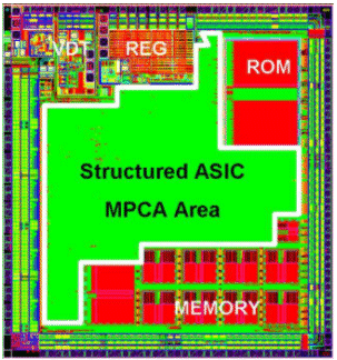
Additionally, customers are able to create their own exclusive platforms according to application-specific requirements. FIGURE 10 shows the layout view of the storage platform, which is co-developed by Faraday and a customer, where MPCA logics can be reconfigured to meet different FLASH memory specifications. This platform can be re-used for the various generations of products.
Figure 9: The layout views of DisplayComposer and NetComposer

Figure 10 The layout views of customer own storage platform

4. Conclusion
The structured ASIC technology is being used as a new approach to ASIC designs, which can cut down NRE cost, and also offer an impressive reduction in time-to-market. We have developed two structured ASIC technologies MPCA and MPIO. Based on these two technologies, Faraday has proposed two structured-ASIC-based solutions TEMPLATE and COMPOSER for platform-based SOC solution. With the aiding of the TEMPLATE and COMPOSER, the implementation of complex SOC designs can be achieved easily and quickly.
Reference
[1] Kun-Chen Wu and Yu-Wen Tsai, “Structured ASIC: A Revolution or an Evolution,” in Proc. International Symposium on Physical Design (ISPD), pp. 103-106, 2004.
[2] “RapidChip™ Integrator Platform ASIC Family Datasheet”, LSI Logic, July 2004.
Related Semiconductor IP
- UFS 5.0 Host Controller IP
- PDM Receiver/PDM-to-PCM Converter
- Voltage and Temperature Sensor with integrated ADC - GlobalFoundries® 22FDX®
- 8MHz / 40MHz Pierce Oscillator - X-FAB XT018-0.18µm
- UCIe RX Interface
Related Articles
- System CoreWare Based Design using RapidChip Platform ASIC
- Structured ASIC Based SoC Design
- NetComposer-II: High performance Structured ASIC Programmable NPU platform for layer 4-7 applications
- EDA in the Cloud Will be Key to Rapid Innovative SoC Design
Latest Articles
- Enabling RISC-V Vector Code Generation in MLIR through Custom xDSL Lowerings
- A Scalable Open-Source QEC System with Sub-Microsecond Decoding-Feedback Latency
- SNAP-V: A RISC-V SoC with Configurable Neuromorphic Acceleration for Small-Scale Spiking Neural Networks
- An FPGA Implementation of Displacement Vector Search for Intra Pattern Copy in JPEG XS
- A Persistent-State Dataflow Accelerator for Memory-Bound Linear Attention Decode on FPGA