Mixed Signal Drivers for Ultra Low Power and Very High Power Applications
Avnet ASIC Israel Ltd. (AAI) - Tel Mond, Israel
Abstract:
Evolving niche markets, such as ICs for biomedical applications, are very challenging in respect to power consumption and on chip power dissipation, namely, wide range from ultra low power (ULP) functionality (<uW) where IC is battery powered, e.g. mobile micro transducers, to very high power (VHP, >5W), e.g. coded energy transfer from RFID¡¯s for remote sensing and animal tracking.
Therefore there is strong need for IC¡¯s operation at wide range of power supply levels: From under 1V battery to above 50V VDS_Max (drain source voltage).
To meet these special requirements a two folded design-fabrication effort is required:
- Foundry device offering should include special oriented device and technology support e.g. LDMOS for high power/voltage operation with its accurate and reliable device models,
- Special in-lab testing procedure should be developed to control and characterize weak LDMOS phenomena as:
- Strong process dependent Vth,
- IDS leakage modeling at elevated VDS conditions,
- Modeling of device self-heating in elevated bias conditions.
With sub-threshold devices operating in ultra low power, special effort is required from foundries to provide devices with superior noise immunity and accurately expanding their models to accommodate for device operating in sub-threshold region.
Foundry should also maintain and provide design guides for good physical realization, high noise immunity and life time device reliability.
As these requirements impose special device support from the IC manufactures. it also requires careful and innovative design ideas from the mixed signal designers [1].
Avnet ASIC Israel Ltd. (AAI) recently designed a group of ULP and VHP mixed signal line drivers IPs using MHS Electronics foundry SCMOS3 process suitable for very high and ultra low power applications.
These IPs are available for customers in need for easy proof of concept by MHS Electronics test chip vehicle, enabling rapid design and manufacturing cycle time. The mixed signal prototypes can be realized using MHS Electronics 10sq.mm Multi-Project Wafer service (MPW) and/or Multi-Layer Mask (MLM 2 or 4 layers per mask).
This approach may also minimize design risks and design verification effort.
MHS Electronics SCMOS3 base line technology is a standard 0.5um mixed signal CMOS process which incorporates the following derivatives:
- Embedded memory process (EPROM/ E2PROM),
- Radiation tolerant (60kRad to 300kRad),
- High voltage high efficient power LDMOS devices [2] (Up to 50V VDS_ Max),
- High value resistors and capacitors.
In the following sections we will cover both foundry and design related issues. Implementation of ULP/VLP line drivers utilizing MHS Electronics SCMOS3 foundry service offering will be demonstrated.
Sections I, II and II (in this precise order) represent the sequent hierarchy: Device ¡ú Circuit ¡ú System.
Section I will cover high power LDMOS device realization and modeling.
Section II will illustrate ULP and VLP design concepts.
Section III will cover system design issues in low powering of logic standard cell library and memory IPs.
Section I: High Power, High Voltage LDMOS Device Realization and Modeling
The PLDMOS device is a symmetric linear P channel with extended Pbody drain. The highest allowed operating voltage on the drain is Vds_max=50V.
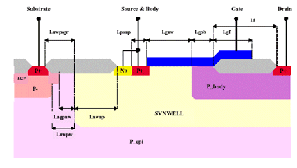
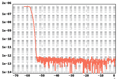
Figure 1. TPLDOX1050: Cross Section and Breakdown Voltage Characteristic @27C
The NLDOMS isolated device is a linear symmetric N-channel transistor with double implanted extended N-drain.
Highest allowed operating voltage on the drain is Vds_max=30V where Vssub_max=60V. This increased breakdown voltage is due to reduced doping level near the PN junction while field oxide is applied to protect the gate from high electrical field.
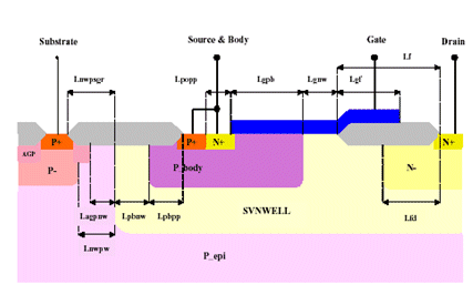
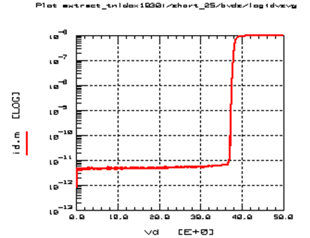
Figure 2. TNLDOX1030i: Cross Section and Breakdown Voltage Characteristic @27C
To define the limits of the Safe Operating Area, the point at ib=cst that gives the minimum value of Vds_max is considered. For Vds lower than Vds_max, the lifetime of the device is guaranteed whatever the Vgs between 0 and Vgs_max. Moreover, the accuracy of the models is guaranteed in this area.
In the transient mode area, drain voltage is allowed to be higher than Vds_max, but for less than few minutes. However, special restriction for Vgs_max may exist. Model precision is not guaranteed in this area.
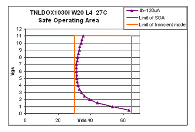
Figure 3. TNLDOX1030i: Safe Operation Limitation Curve Example
Section II: Very High and Ultra Low Power Line Drivers
VHP: For typical high power application there is a need to deliver >5W (rms) to external load.
The suggested line driver uses push-pull amplifier utilizing complimentary LDMOS devices. The electrical specifications of these two devices were given in Section I.
To achieve minimum on chip power dissipation and efficient power delivery, a special care is given for impedance matching and power device R_on resistance. Slew rate control and timing alignment between pre-driver rising edge and falling edge should be realized to minimize overlap and zero crossover distortion. Consequently lower chip dynamic current and charge build up at transformer can be guaranteed over all process corners.
Impedance matching and proper Timing is controlled in low voltage digital domain while level shifter pre-driver circuitry provides the precise high power driving levels. In this example level shifting from 40V to 50V for the P_LDMOS device and 0V to 10V to the N_LDMOS device can be achieved.
Device R_on is controlled by low voltage logic configuration of device sizing followed by high voltage level shifters and pre drivers. For <4 Ohm R_on, the required physical (layout) device is 0.3 sq.mm. Figure 4 is a schematic view of full bridge configuration [3] VHP driver with its pre-driver level shifter and load together with its simulated transient behavior.
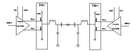
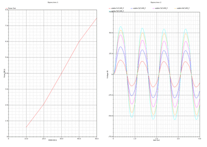
Figure 4.
(a) Very High Power Line Driver and External Resonance Network
(b) Transient Simulation of Voltage and Power Output at Load Terminals
As indicated in Fig. 4b maximum power greater than 7W can be delivered with efficiency greater than 70%, due to its low Driver R_on and low zero cross over distortion.
The level shifter analog block is shown in Fig. 5. with its simulated transient behavior. It converts low level voltage signal (0 - 5V) to an equivalent high level voltage signal (0 - VDDH).
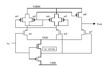
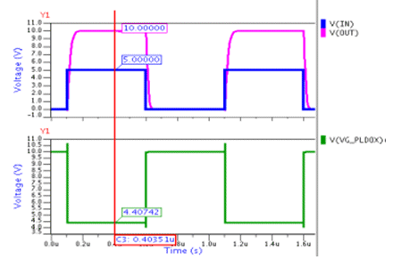
Figure 5.
(a) Very High Power Line Driver and High Voltage Level Shifter
(b) Voltage Transient Simulation
The proposed level shifter [4] circuit input is Vin, circuit output is Vout. VDD is the 5V low voltage supply and VDDH the high voltage supply. PMOS LV transistors are m3, m2, m6 and m5. NLDOX10 transistors are m1, m4, and m7. PLDOX10 transistor is m8. SC_INVX8 is an inverter (1 TNLV + 1 TPLV) from design kit scmos3ee standard cells library.
Design concept: m7 and m8 transistors work like usual CMOS structure. NLDOX10 transistor (m7) is activated with respect to GND where PLDOX10 transistor (m8) is activated with respect to VDDH. The potential difference VGS of m8 transistor can not be greater than 11V, a voltage level shifter is necessary to drive the m8 transistor. This voltage level shifter is made by m3, m2, m6 and m5 transistors. From 0V input voltage, it generates an output voltage equal to VDDH - 5V on m8 transistor, from 5V input voltage; it generates an output voltage equal to VDDH on m8 transistor.
ULP: Typical low power application allows < 10uW power consumption from <2V ±5%, 10mAhour battery. Thus it will require on chip charge pump circuitry to supply the ULP line driver. A typical low power application is illustrated in Figure. 6. Here in response to biological event, a short burst of few mA current pulses are triggered in this half bridge configuration between VCCH and El2 electrodes (e.g. Antenna Coil in RFID tag). Therefore a high regulated voltage should be supplied by a charge pump circuitry.
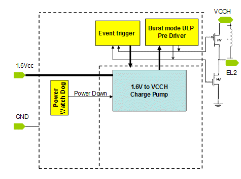
Figure 6. Typical Low Power Application
Typical charge pump circuit consists of:
- Power switches,
- Comparator,
- Non-overlapping clock generator,
- Resistive divider,
- High value decoupling and flying Capacitors.
Excluding higher than 10nF capacitors, all components can be realized on chip using LDMOS as power switches and level shifters for possible high voltage systems requirements (e.g. high voltage level sensing/controlling).
The charge pump regulated voltage is feeding the ULP push pull line drivers.
Non-overlapping cloak generator and glue logic should be operated near sub-threshold region where special care is made to minimize noise impact on sub threshold device functionality.
Isolated source devices like TNLDOX1030i provide better noise immunity than non-isolated source devices.
Section III: Low Powering of Logic Standard Cell and Memory IPs
MHS Electronics SCMOS3EE Logic Standard cell library is characterized to operate with power supply 5V (+_10%) to 2V (+_10%). In operation down to 1.8V it enables switching power saving and DC power saving by more 8X in respect to 5V operation.
EPROM and E2PROM IP blocks include control logic, chare pump and Buffers coming in various 8it/16Bit Capacity (2k to 64k), in sizes of down to 0.4mm2 and less than 3uA Standby consumption.
For low power applications several techniques are used to reduce switching power such as:
- Automatic clock gate insertion by the synthesis tool,
- Manual clock gating insertion for different operation modes and for memories,
- Manual data and address gating,
- Manual clock gate placement for clock tree roots. At typical application allowing 0.5nS slope on 50MHz clock sinks, this technique can save up to 0.25mA or 33% of total consumption. These numbers were extracted from the example structure shown at Figure 7, where load wire 1mm x 2um was equivalently simulated as 0.1pF and 25 Ohm. The en/clk load ratio is 25%.
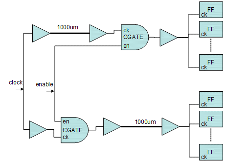
Figure 7. Clock Gating Example
Leakage power is reduced by separate power domains that can be switched off by power switches. Basically an Always-On domain is used to maintain functionality in standby mode and turn on the other power domains when required.
The signals to and from the powered down domain need to be set to correct logic values during power down with isolation gates.
If the powered down logic contains sequential logic and memory elements whose data should be kept during power down a third power retention domain can be introduced. In standby mode the power retention domain is kept at reduced VCC level by x4 to x16 , which is enough to keep the sequential logic and memory values unchanged[5]
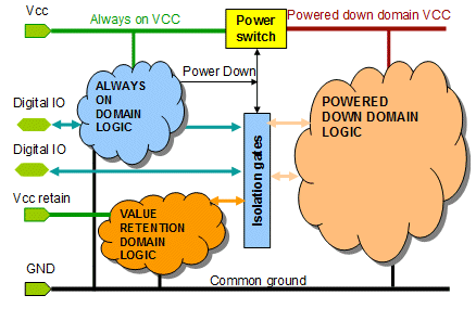
Figure 8. Power Domains Switching
Summary
In many biomedical applications the need for either Ultra low power consumption ICs or Very high voltage device capabilities imposes challenges both on IC foundries manufactures and mixed signal designers.
AAI and MHS Electronics are offering unique solutions to these challenges whereas MHS Electronics fabricates competitive LDMOS devices in embedded memory standard CMOS process and AAI provides state-of-the-art System-on-Chip design methodologies.
The basic approach demonstrated here enables the design and manufacturing of low cost ICs for specific applications among which are:
- Industrial control,
- Ultra low power biomedical devices,
- High¨Cside switching applications,
- High voltage LED display/Lamp drivers,
- Solenoid drivers,
- High voltage FOR MEMS applications,
- Radiation tolerant devices,
- Smart Cards and RFIDs.
[1] Dong Pan, Harry W. Li and Bogdan. M., "A Low Voltage to High Voltage Level Shifter Circuit for MEMS Applications¡± Microelectronics Symposium, 2003. Proceedings of the 15th Biennial.
[2] Rinaldo Castello, Ferdinando Lari, Marco Siligoni and Luciano Tomasini, ¡°100-V High-Performance Amplifiers in BCD Technology for SLIC Applications¡±, IEEE J. of Solid State Circuits, Vol. 27, No 9 Sep92.
[3] Edoardo Botyi, Tiziana Mandrini and Fabrizio Stefani, "A High-Efficiency 4 x 20 W Monolithic Audio Amplifier for Automobile Radios Using a Complementary D-MOS BCD Technology¡± IEEE J. of Solid State Circuits, Vol. 31, No 12 Dec96.
[4] Bruno Villard¡®s thesis ¡°Réalisation de structures haute tension á partir d¡¯un procédé CMOS 0.7 microns". 1997
[5] Standby Power Reduction using dynamic voltage scaling and canary flip-flop structures Calhoun B.H. ; Chndrakasan, A.P., IEEE Journal of Solid-State Circuits, Volume 39, Issue 9, Sept 2004, 1504 - 1511
Related Semiconductor IP
- xSPI Multiple Bus Memory Controller
- MIPI CSI-2 IP
- PCIe Gen 7 Verification IP
- WIFI 2.4G/5G Low Power Wakeup Radio IP
- Radar IP
Related White Papers
- Mixed Signal SoC Applications
- It Takes tools to Raise a Programmable Mixed Signal SOC
- Reuse of Analog Mixed Signal IP for SoC Design: Progress Report (Cadence Design Systems)
- Die-level process monitor for mixed signal designs