Fast Design Productivity for Embedded Multiprocessor through Multi-FPGA Emulation: The case of a 48-way Multiprocessor with NOC
Abstract:
Design productivity is one the most important challenge facing future generation multiprocessor system on chip (MPSOC). The modeling of dozens of interconnected IPs with distributed memories implies intensive manual EDA based design activity. We propose to improve design productivity by raising IP reuse to small scale multiprocessor IP combined with fast extension techniques for system level design automation in the framework of multi-FPGA based emulator. A design case study of a 48-processors multiprocessor on 4 large scale FPGA based industry class emulator validates our approach.
I. Introduction
ITRS Semiconductor roadmap [1] projects that hundred of processors will be needed for future generation MPSOC designs. Among the various challenges of MPSOC [2] design productivity with design constraints is paramount.
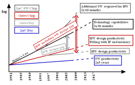
Fig. 1 – ITRS 207 Design productivity gap
Design productivity of large scale multiprocessors is first affected by the EDA based design effort that is combining hundreds of IPs followed by fast and efficient design space exploration. Designing large scale multiprocessors based on small scale
Multiprocessors allow to quickly duplicate building elements and build a large scale multiprocessor in short design time. We propose in this paper a multiprocessor design methodology which allows fast design productivity based on a small scale multiprocessor IP for reuse in large scale multiprocessors and multi-FPGA emulation for fast validation and performance evaluation.
II. Multi-processor Architecture
A. Overall Architecture
Our target architecture is a 48-processor multiprocessor organized as a 4x4 mesh of clusters fully interconnected through a network-on-chip (NOC). Each cluster includes 3 processor elements and a local memory connected to a NOC switch. The architecture is symmetrical which makes it a good candidate for design modularity and IP based design and reuse.
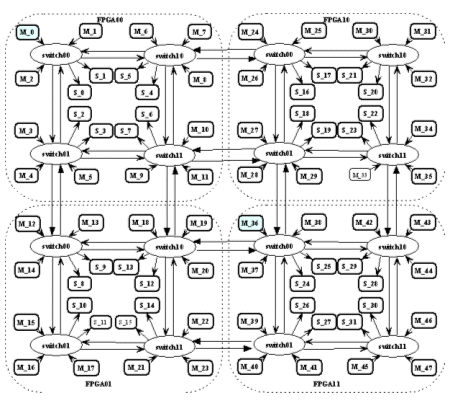
Fig. 2 – Target 48-processors multiprocessor architecture
In order to achieve fast design productivity for this target architecture we need: (1) to raise the level IP design and reuse to Small Scale Multiprocessor (SSM IP) and automatically duplicate and adjust NOC characteristics to reach the desired size (2) fully integrate all EDA tools involved in the design (3) due to its large size and prohibitive simulation time at RTL level, we need emulation for the validation, test and performance evaluation of this multiprocessor architecture. In addition emulation requires synthesis place and route which provides accurate area and maximum operating frequencies data. Our methodology will exploit the concept of FPGA IP which is the maximum size modular IP which can fit in a single FPGA device of the emulation platform and which can be duplicated. This requires a prior analysis of the emulation platform and the FPGA devices used in it.
Our emulation platform is the Eve Zebu-UF4 Platform [10-14].
B. Emulation : Eve Zebu-UF Platform
The ZeBu-UF4 emulator platform is based on 4 Xilinx Virtex-4 LX200 devices placed on an extended PCI card via a motherboard-daughter card approach.
TABLE I: EVE ZEBU-UF4 PLATFORM DETAILS
| Modules | Descriptions |
| FPGA | 4 Virtex-4 LX200 |
| DRAM | 512 MBytes |
| SSRAM | 64 MBytes |
| ICE | Smart and Direct |
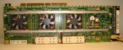
Fig. 3 - Eve Zebu-UF4 Platform.
The 4 FPGA based system can emulate the equivalent of up to 6 million ASIC gates in a single system. ZeBu-UF4 also includes on-board memory capacity based of 64 MBytes of SSRAM and 512 MBytes of DRAM memory chips via an additional memory board, which plugs into the PCI motherboard. The ZeBu-UF4 emulation system can be used in various ways such as co-emulation with commercial HDL simulator, co-emulation with both transaction level and signal-level SystemC and with synthesizable test bench. Performance ranges for these various uses are given in Table II.
TABLE II: EVE ZEBU-UF4 OPERATING MODE AND PERFORMANCE
| Operating Mode | Performance Range |
| Max capacity in ASIC gates | 6M |
| Co-emulation with commercial HDL simulator | 5K-100KHz |
| Co-emulation with signal-level C/C++/SystemC | 100K-500KHz |
| Co-emulation with transaction-level C/C++/SystemC/SystemVerilog | 500K-20MHz |
| Test vectors | 100K-500KHz |
| Emulation with synthesizable test bench | <=20MHz |
| In-circuit emulation, connected to target system | <=20MHz |
| Emulation with SW debuggers via JTAG interface | <=20MHz |
C. IP Design and reuse
This important multiprocessor architecture requires efficient IP design and reuse. Although we use Xilinx EDA tools and IPs for the Xilinx target Virtex-4 LX-200 no multiprocessor soft IP is available which matches our need. The Multiprocessor can be built through increasing size small scale multiprocessor IP: (1) single switch based (2) 2 switches based and so on up to the full capacity single LX200 FPGA reuse.
TABLE III: IPS FOR MULTIPROCESSOR DESIGN
| IP component | Description | Source | Version |
| Processor | Soft core IP | MicroBlaze Soft core IP Xilinx | 5.00 b |
| Memory | Soft core IP | Xilinx Coregen 96KB | v.2.4. |
| Network on chip switch | Soft core IP | VHDL Arteris Danube library | 1.10 |
| Interchip | Soft core IP | VHDL Arteris Danube library | 1.10 |
In our application we will use the emulator with synthesizable test bench.
III. Design Automation and IP Issue
This main approach requires EDA tools combination and integration. We first introduce Eve Zebu design flow.
A. Eve Zebu Design Flow
The Design Under Test (DUT) is mapped onto one or several FPGAs and memory chips. The mapping is carried out through any one of the most popular commercial ASIC/FPGA RTL synthesis tools plus the ZeBu software compilation package to deal with the DUT gate-level clustering, and clock and memory modeling. The Zebu design flow is given in figure 6. All the system EDIF files generated by synthesis are used by Zebu compiler for the implementation on FPGAs. The compilation is incremental but the Xilinx ISE P&R phase can be parallelized to reduce the turnaround time.
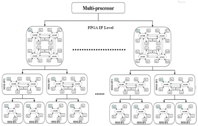
Fig. 4 –Small Scale Multiprocessor IP Reuse and Automatic Composition
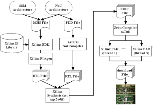
Fig. 5 - Workflow of Multi-FPGA MPSoC
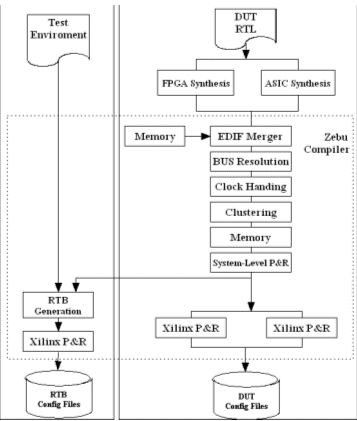
Fig. 6 - ZeBu Compilation Flow Overview.
Once the design and the test environment have been mapped, ZeBu provides a comprehensive, efficient and high-performance hardware or software test environment for the emulated DUT.
B. EDA Tools Integration
Design automation tools of 3 commercial companies are combined together to generate our multi-FPGA MPSoC. Figure 5 describes the workflow. The Xilinx EDK [7] tool is used to generate our SSM multiprocessor using Xilinx IPs. Once the RTL files of SSM are generated, they are reused for the multi-FPGA large scale multiprocessor synthesis, which can largely reduce system design time. Different NoC files are synthesized for each SSM on different FPGA chips of Zebu platform by changing the generic route-table according to the XY routing algorithm and the SRAM addresses on each FPGA. These NoC RTL files are generated by Arteris NoCcompiler tool [5], which allows the export of NoC using the Arteris Danube Library [6]. Eve Zebu compiler [12] takes the EDIF files converted by Xilinx synthesis tools for the implementation. Different SSM IPs are analyzed and distributed onto FPGAs. User constraints can be used to accelerate this incremental process. Finally Xilinx place and rout tools are used to generate the download bit files of FPGA. This phase can be parallelized to reduce the turnaround time. Area and performance results are obtained.
C. Small Scale Multiprocessor IP
The architecture of the small scale multiprocessor is based on a mesh-based network on chip connecting 12 processors organized as with 3 processors and 2 SRAM on chip memories per switch. The network on chip topology is mesh for a better multi-FPGA implementation. This small scale multiprocessor represents a 12 processors single chip multiprocessor which is representative of current small scale multiprocessor on chip.
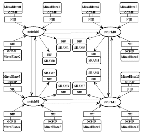
Fig. 7 – 12 Processors OCP-IP connected Small scale multiprocessor IP (SSM IP)
TABLE IV: IP NUMBER OF SMALL SCALE MULTIPROCESSOR
| IP component | Qty |
| Processor | 12 |
| Memory | 12 |
| Network on chip switch | 4 |
| Interchip | 1 |
The design is OCP-IP compliant which implies that we can change processor IP by any other OCP-IP compliant processor IP while leaving the overall design identical. The OCP-IP protocol is used for the communication between the processors and Network on Chip (NoC). MicroBlaze soft IP [9] is a 32-bit 3-stage single issue pipelined Harvard style embedded processor architecture provided by Xilinx as part of their embedded design tool kit. The MicroBlaze is flexible, and gives the user control of a number of features such as the cache sizes, interfaces, and execution units like: selectable barrel shifter (BS), hardware multiplier (HWM), hardware divider (HWD), and floating point unit (FPU). A network interface is designed in order to make MicroBlaze compatible to OCP-IP protocol. This interface gets data from MicroBlaze through FSL link and transfers the data to the Network on Chip under OCP-IP protocol. Each MicroBlaze communicates with a 32KB local memory via LMB bus on one side and with the Network Interface (OCP-IP) on the other side.
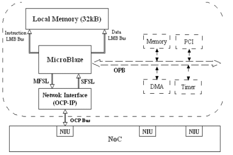
Fig. 8 - Processor Tile
D. Arteris NoC
The design of the network on chip is based on Arteris Danube Library. The Arteris Danube library [6] includes the switch generator which is an essential building block of the NoC interconnect system. The main features of Arteris switch are: (1) fully synchronous operation, (2) internal full crossbar: up to one data word transfer per MINI port and per cycle, (3) full throughput arbitration: up to one routing decision per input port and per cycle, wormhole routing to reduce latency (4) freely cascading connection, supporting any loop-less network topology. It is possible to select the arbitration type of the switch among 4 possible values Round-Robin, LRU, Random, and FIFO with default value round robin. Several optional registers can be added in order to pipeline the switch.
IV. Performance Evaluation
As a first application we evaluated a simple parallel software example the dot product. Each PE tile calculates a dot product of dimension 800*800. All the variables are floating point numbers to show the impact of FPU units. A global synchronization is used to make sure all the computations are finished.
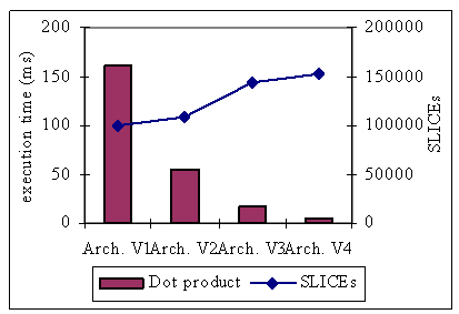
Fig. 9 - Execution time of Dot Product.
We generated 4 different architectures (V1, V2, V3 and V4) with varying micro-architecture characteristics. For example the floating point unit (FPU) can greatly improve the performance of MicroBlaze and the pipelines of NoC switch options can improve the system timing. This illustrates the capacities of design space exploration based on this multi-FPGA emulator platform. Clearly the 4 architectures have varying execution times and area implementation requirements. Between best and worst in area the factor is 153 % while performance factor is 2798 %. Our next step is the fully automatic design space exploration of emulator based multiprocessor design.
V. Conclusion
Design productivity for large scale system on chip is a major challenge. Multiprocessors system on chip design can benefit from: (1) larger IP design and reuse such as small scale multiprocessor IP (2) multi-FPGA emulation platforms for quick and modular duplication combined with fully integrated EDA tools. We proposed a small scale multiprocessor design as a building block for large scale multiprocessor. This SSM IP can be quickly extended in order to build larger scale multiprocessor. We validated our approach on a 48 processors system by automatically extending a 12 processors small scale multiprocessor IP. Several large scale software applications (e.g. cryptography, software defined radio) are currently developed to be ported on this platform.
Acknowledgment
We are grateful to EVE team for their support and collaboration.
REFERENCES
[1] ITRS
[2] A.A.Jerraya and W.Wolf, “Multiprocessor Systems-on-Chips”, Morgan Kaufman Pub., 2004.
[3] N. Genko, D. Atienza, G. De Micheli, J. M. Mendias, R. Hermida, F. Catthoor, A Complete Network-On-Chip Emulation Framework, Proceedings of the conference on Design, Automation and Test in Europe Volume 1 DATE '05, March 2005
[4] Arteris S.A.
[5] NoC Solution 1.10, NoC Compiler user's Guide, o918v2rs4, Dec. 2008, Arteris
[6] Danube 1.10 – Packet Transport Units Technical reference – 04277v3rs6 – March 2008, Arteris.
[7] Xilinx. Embedded system tools guide.
[8] Xilinx. Xilinx fast simplex link IP.
[9] Xilinx. Xilinx MicroBlaze soft core processor.
[10] ZeBu-UF Product Overview, Document revision – b –, November 2005, EVE.
[11] ZeBu-UF Installation Manual, Version 4.3_x, May 2008, EVE.
[12] ZeBu-UF Compilation Manual, Version 4.2_x, December 2007, EVE.
[13] ZeBu-UF Reference Manual, Version 1.3_x, February 2006, EVE.
[14] The ZeBu-UF Tutorial, Version 4.2_x / 4.3_x, March 2008, EVE.
Related Semiconductor IP
- NPU IP Core for Mobile
- NPU IP Core for Edge
- Specialized Video Processing NPU IP
- HYPERBUS™ Memory Controller
- AV1 Video Encoder IP
Related White Papers
- Multi-FPGA NOC Based 64-Core MPSOC: A Hierarchical and Modular Design Methodology
- 3D IC 2-tier 16PE Multiprocessor with 3D NoC Architecture Based on Tezzaron Technology
- Soc Design -> Emulation verifies multiple network interfaces
- SoCs: DSP World, Cores -> 3G wireless SoC requires emulation
Latest White Papers
- Ramping Up Open-Source RISC-V Cores: Assessing the Energy Efficiency of Superscalar, Out-of-Order Execution
- Transition Fixes in 3nm Multi-Voltage SoC Design
- CXL Topology-Aware and Expander-Driven Prefetching: Unlocking SSD Performance
- Breaking the Memory Bandwidth Boundary. GDDR7 IP Design Challenges & Solutions
- Automating NoC Design to Tackle Rising SoC Complexity