Multi-FPGA NOC Based 64-Core MPSOC: A Hierarchical and Modular Design Methodology
Abir M'zah and Omar Hammami
ENSTA ParisTech
Abstract :
With the increasing need for real time complex applications, number of processors in the same MPSOC design is becoming a critical parameter to evaluate its performance. As a first step, we design a 2Ary-4Fly NoC with 16 masters and 16 slaves. Based on this NoC, we design an hierarchical architecture with one central NoC connecting 4 similar NoCs modules. This one is implemented on different FPGAs (virtex4-LX-200) of the board Zebu-UF4. This architecture gives the possibility to the 64 processors to share 4 BRAMs situated on the high level NoC. This hardware is suitable for parallel programming with heavy computational algorithms.
I. INTRODUCTION
MPSOC is an emerging technology allowing the building of an entire system on a single chip. With the flexibility given by the use of the Network On Chip, several industrial chips are designed with a NoC and multi processors. For example, the chip 81.6 GOPS [1] is a MPSOC including a central NOC and 10 processors designed for mobile intelligent robot applications. The MAGALI [2] platform is also a heterogeneous NoC-based MPSOC for Mobile Terminal in 65nm low-power CMOS. The ARM Cortex-15 processor [3] with its advanced structure (figure 1) is expected to deliver over 5 times the performance of today‟s advanced smart phone. The MIPS32 1074K [4] Coherent Processing System (CPS) is the latest coherent multiprocessor IP offering from MIPS Technologies. This CPS is available as fullysynthesizable multicore IP that achieves high frequencies using commercially-available, noncustom, standard cells and memories. TILERA presents also its multicore processor family which is TILE64[11]. This one presents 64 processors interconnected with TILERA‟s mesh NoC.
In this work, we will implement a hierarchical design based 64-Core with NoC modularity. For this, we use the zebu-UF4 [6] platform with its 4 FPGAs virtex4-LX200. In the next section we present the basic NoC architecture. In section 3, we present the new extended project with a central NoC. Section 4, will be the subject of the workflow presentation. In section 5, we will present the implementation results on the Multi FPGA platform. We conclude in the last section.
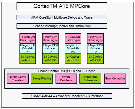
Figure 1. ARM Cortex-15 Block Diagram
II. NOC 2-ARY 4-FLY DESIGN
In this section, we present the design of a NoC with 16 masters 16 slaves with the topology 2Ary- 4Fly presented in figure 2. We use Arteris NoC solution [7] to design this NoC. First, we create an OCP [8] initiator which will be used for all masters and an OCP target for slaves. To connect each master to a switch we need an interface wrapper which is an OCP-to-NIU structure. Each couple of OCP-to-NIU interface is connected to a switch from the stage 1. All the switches of this architecture have a degree equal to 4. Table 1 presents the switch‟s properties used in this design. The connection between switches is respecting the butterfly topology. In the last stage, we need also NIU-to-OCP interfaces to connect switches to the slaves. Once the architecture of the NoC becomes ready, routing tables take the task to ensure the transfer of data between masters and slaves. In fact, each switch of this NoC is associated to its specific routing table. Thanks to this one, a switch is able to send data to the specific output port (TX0 or TX1).
TABLE I. SWITCH PROPERTIES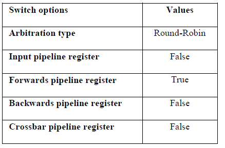
We suppose that master 0 wants to send a command to slave 5. The Head of the data packet contains the address of the slave 5. To simplify the work, we affect to each slave a global address beginning with its range in hexadecimal for example slave 2 has an address equal to 200000 , slave 10 has an address equal to A00000. Data Packet which will be sent from master 0 to slave 5 has an address beginning with 5. When the packet reaches switch 1.0, this one will check its routing table and decide to send it to the switch 2.2 through the output TX1.When the Switch 2.2 receives the packet, it sends it to switch 3.2 through its TX0. The switch 3.2 notes that packet with address beginning with 5 has to be sent through its Tx1 to finally reach its slave destination as shown in Figure 1.
III. MODULAR AND HIREARCHICAL DESGN
In figure 3 we present the extended design which is based on the NoC described in the previous section. In fact, we use 4 NoCs having the same architecture. The benefit of this project is to give the 64 processors from any local NoC the possibility to access the same shared memories situated on the central NoC. For each NoC we sacrifice one slave, to connect it to the high level NoC, the other slaves are BRAMs blocks memories. Each processor can send data to the central memories through slave 16. This hardware project is suitable for heavy computational applications. We can store data like images in the shared memories, in this case each processor can access it and make its local analysis then stores the result in another memory.
In this work, we use Xilinx tools : EDK with version 9.20.2i to create a project where we integrate the NoC as an IP. As masters, we choose to use Microblaze [9] processors. Each Microblaze is connected to its local memory BRAM through two buses. DLMB (Data Local Memory Bus) is the responsible of data transfer between the local memory and the microblaze. In the other hand, the ILMB (Instruction Local Memory Bus) ensure the transfer of instructions from the microblaze to the BRAM. We can add FSL ports to this processor when we need to make a connection with an FSL (Fast Simplex Link). We add the 4 NoCs as IPs in the EDK project to connect the 64 Microblaze which are the masters to 60 blocks memories representing the 15 slaves. To evaluate the execution time of the design we add a timer which is connected to an OPB (On-Chip Peripheral Bus). To connect each master to the network we need an interface wrapper between the FSL port and the OCP input of the network. For this, a homemade interface called FSL2OCP was designed in our team which plays the role of an adapter between the FSL link and the OCP input. We use two interfaces an OCP-to-NIU and an NIU-to-OCP. The output of our NoC will have the OCP type, so to connect it to the memory slave we use an OCP2bram interface. All the hardware components used in this project, are presented in the table 2.
TABLE II. USED IPS VERSION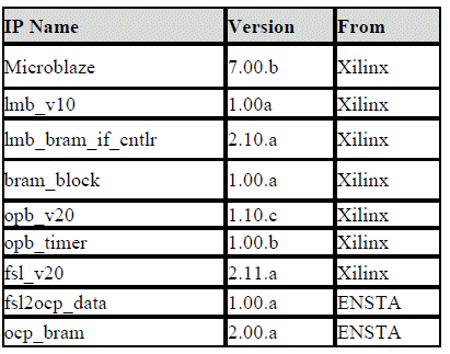
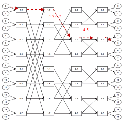
Figure. 2. 2-Ary 4-Fly topology
Click to enlarge
Figure. 3. Hierarchical NoC Design
V. DESIGN METHODOLOGY
Even though in this work we only did the hardware part, we will present all the workflow from the hardware conception to the board execution (figure 4). After the generation of the netlist of the project, we use the command ngc2edif to transform the netlist to edif files. ZCui is a compiler tool designed by EVE company [6] to synthesize the DUT (Design Under Test) by calling Xilinx tools. At the end, it generates a bit file and several reports describing the FPGA resources used after the placement and routage on the board. For each microblaze, we can create a software application in the EDK project. For each application we add a C code and header files to describe the tasks affected to each processor. Once we define the 64 applications, EDK calls C code compiler and generates *.elf files. We transform these files to *.vhex files which can be run on the board. At this level we have now hardware and software files ready to be run on the zebu board. We call the command zRun to make the execution on the board. Eve tool offers the possibility to use static and dynamic probes. In our case we use static probe to capture the end of the execution time. In fact, the run will stop when the condition of stop which is related to the probe value will be true. Then we can read the execution time needed for the program to be complete.
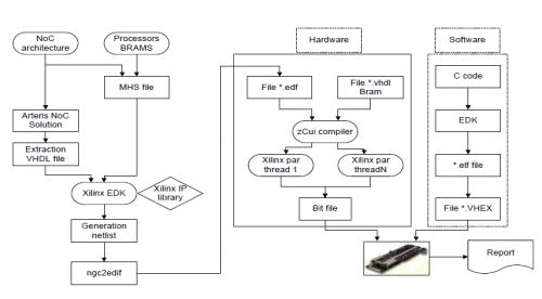
Figure. 4. Workflow design presentation
V. SYNTHESIS RESULTS
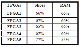
We use Zcui compiler which is a software of EVE company[6], to make the synthesis , the placement and the routage on different FPGAs. We can choose in the zCui compiler the Clustering options. In our case, we use the full automatic clustering, that is why this tool will try to share the netlist between FPGAs with equal rates. We can see synthesis results in table 3. We use more then 66% of Slices in all the FPGAs. Resources in term of memories are also used with a percentage of 66% for 4 FPGAs and 55% for the 5ith.
TABLE 3. RESOURCES UTILIZATION
VI. CONCLUSION
In this work we designed a hierarchical 64 PE based NoC architecture. At the first step we used Arteris NoC Solution [7] to design a NoC with 16 masters and 16 slaves with the topology 2Ary 4Fly. This NoC is then considered as the basic module of our new hierarchical NoC design. In fact, we use 4 similar NoC modules interconnected with a high level central NoC.
We present the results of the synthesis and the implementation on a multi FPGAs platform zebu UF4. This Design needs 5 FPGAs Virtex 4 LX 200 to be implemented on. In the future work we will develop an application suitable for this hardware which can be an image processing program.
REFERENCES
[1] K. Donghyun and K.Kawanho, “81.6 GOPS Object Recognition Processor Based on a Memory-Centric NoC”, Congres International Symposium on Networks-on-Chip (NOCS), 2009, vol. 17, no3, pp. 370-383
[2] F. Clermidy, R. Lemaire, X. Popon, D. Kténas and Y. Thonnart, ”An Open and Reconfigurable Platform for 4G Telecommunication: Concepts and Application”,” Euromicro Conference on Digital System Design (DSD), Aug. 2009,pp, 449 – 456
[3] http://www.arm.com/products/processors/cortex-a/cortexa15.php
[4] http://www.mips.com/media/files/MIPS32_1074K_910.pdf
[5] X.Li and O.Hammami,” Fast Design Productivity for Embedded Multiprocessor through Multi-FPGA Emulation: The case of a 48-way Multiprocessor with NOC „‟,2009 OCP-IP Newsletter , http://www.design-reuse.com/articles/24448/16penoc-based-multi-core-synchronization-mechanisms.html
[6] EVE TEAM Zebu-UF Emulation platform. www.eveteam.com
[7] Arteris S.A. http://www.arteris.com
[8] OCP-IP Open Core Protocol Specification 2.2.pdf http://www.ocpip.org/ , 2008
[9] Xilinx microblaze soft core processor. Available on: http://www.xilinx.com/support/documentation/index.htm.
[10] Z.Wang, and O.Hammami, “External DDR2-constrained NOC-based 24-processors MPSOC design and implementation on single FPGA”, Design and Test Workshop, 2008. IDT 2008. page(s): 193 – 197, 2008.
[11 http://www.tilera.com/sites/default/files/productbriefs/PB010_TILE64_Processor_A_v4.pdf
Keywords- Multi-FPGA; Network on Chip; hierarchical ; modules ; MPSOC
Related Semiconductor IP
- UFS 5.0 Host Controller IP
- PDM Receiver/PDM-to-PCM Converter
- Voltage and Temperature Sensor with integrated ADC - GlobalFoundries® 22FDX®
- 8MHz / 40MHz Pierce Oscillator - X-FAB XT018-0.18µm
- UCIe RX Interface
Related Articles
- Prototyping Mesh-of-Tree NOC Based MPSOC on Mesh-of-Tree FPGA Devices
- An HDTV SoC Based on a Mixed Circuit-Switched / NoC Interconnect Architecture (STBus/VSTNoC)
- Fast Design Productivity for Embedded Multiprocessor through Multi-FPGA Emulation: The case of a 48-way Multiprocessor with NOC
- Performance Measurements of Synchronization Mechanisms on 16PE NOC Based Multi-Core with Dedicated Synchronization and Data NOC
Latest Articles
- An FPGA-Based SoC Architecture with a RISC-V Controller for Energy-Efficient Temporal-Coding Spiking Neural Networks
- Enabling RISC-V Vector Code Generation in MLIR through Custom xDSL Lowerings
- A Scalable Open-Source QEC System with Sub-Microsecond Decoding-Feedback Latency
- SNAP-V: A RISC-V SoC with Configurable Neuromorphic Acceleration for Small-Scale Spiking Neural Networks
- An FPGA Implementation of Displacement Vector Search for Intra Pattern Copy in JPEG XS