Methodology to reduce Run Time of Timing/Functional Eco
By Sunandan Choubey, Himanshu Bansal, Dr. Rajendra Pratap (einfochips (An Arrow Company))
Abstract
Chemical Mechanical Planarization is a process of smoothing wafer surface through exerting the chemical and mechanical polishing on wafer. It is an important step in IC fabrication process. To achieve the planarity of the surface of wafer, dummy metal fills are required to be inserted to have even distribution of the material on the surface. Dummy fill insertion is a time consuming process for moderate and bigger sized blocks or chips. Insertion of Dummy metal fills affects the coupling capacitance of the signal metal layers, which causes signal integrity issues. In the last stages of the design closure while doing Timing ECOs, re-doing Dummy metal fills can re generate timing/noise violations and ECOs can become unpredictable. In this paper, we are suggesting a methodology wherein eco can be implemented without re-running the Dummy metal fill again on the complete block/chip. This will save ECO implementation time and reduce the risk of any new signal integrity issues.
Keywords
CMP (Chemical Mechanical Planarization), ECO (Engineering Change Order), ILD (Inter-Level Dielectric), GDS (Graphic Data System), TCL (Tool Command Language), Crosstalk, Dummy Metal Fill, Coupling Cap, PnR (Place and Route).
1. Introduction
Dummy metal fill insertion, which is done to achieve even distribution of material on the wafer surface and thus planarity on surface between two layers while doing the chemical mechanical planarization. Uneven Inter-level-dielectric (ILD) or features’ thickness can cause deformation of inter level dielectric as shown in Fig.1 (a)
To reduce this variation of Inter-level-dielectric (ILD) on wafer surface dummy metal fills or dummy geometries or dummy features are inserted as shown Fig.1 (b)


Fig.1 ILD planarization due to non-uniform density,
(a) Before dummy metal fill and (b) after dummy metal fill
The Dummy metal fills are not only used for Planarity purpose but also for uniform density, in order to achieve constant thickness across the chip after CMP step. If Dummy metal fills are not inserted or there is non-planarized surface, then further layers being printed may have unpredictable deformities as shown in Fig.2
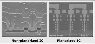
Fig.2 (Non-planarized metals and planarized IC)
Dummy metal filling process have very high runtime and create signal integrity issues like noise due to coupling capacitance with their adjacent signal metal shapes. Dummy Fills are of two types:
- Grounded fills and
- Floating fills.
Grounded fills are used in High-speed designs. It has lager impact on the filling process and it requires power and ground connection to be connected with the fill geometries. This has an impact on the routing resources. On the other hand, floating fills do not require power and ground connections and gives small increase in the total capacitance as compare to the Grounded fills. However, Floating fills increase the coupling capacitance of their neighboring signal shapes. This leads to signal integrity issues such as cross- talk delay and noise.
Crosstalk delay is the undesired change in the speed of electrical signals due to capacitive cross coupling between two adjacent signal nets or between signal net and dummy metal fills.
Crosstalk noise is the undesirable change in the logic level of electrical signals due to capacitive cross coupling between two adjacent signal nets or between signal net and dummy metal fills. It means any undesirable deviation in voltage of a net that ought to have a constant voltage, such as a logic 0 or logic 1. This deviation in voltage is called bump/glitch. This causes incorrect logic to be propagated resulting in functional failure. It is very serious problem.
2. Coupling cap
Ideally, a parallel plate capacitance exists between two metal plates and is separated by a small distance (tdi). The parallel-plate capacitance is given by ![]()
where ![]() is the permittivity of the material separating the two plates,WL is the area of the two plates and tdi is the distance between them as shown in Fig 3.
is the permittivity of the material separating the two plates,WL is the area of the two plates and tdi is the distance between them as shown in Fig 3.

Fig 3 Capacitance
Two same-layer interconnects may be viewed as two parallel plates separated by a small distance. However, the height and width of the plates (interconnects) is not large in comparison to the spacing and thus there is a significant divergence from ideal parallel-plate capacitor behavior. Capacitance is directly proportional to the charge accumulated on one of the electrodes (Q =CV). The charge density on an electrode depends on the electric field close to the electrode (E = σ/WL). Therefore, the electric field close to an electrode determines the capacitance of a configuration. When the Dummy floating fill plates of thickness t are inserted between two conductors, it reduces the distance between the metal plates and increases the capacitance by ![]()
The Coupling capacitance is of two types:
- interlayer and
- intra-layer capacitance
Capacitance existing between two different layer is called intra-layer capacitance and Capacitance existing between two same layers is called inter layer capacitance. Capacitance existing between dummy metal fill and same metal signal layer is also treated as interlayer coupling capacitance.
Coupling capacitance depends on various factors as follow:-
- Shape
- Size
- Spacing
2.1. Fill Shape
Coupling capacitance depends on fill area overlapping with signal metal shapes. If the overlapping area between metal layer and fill is more, than the coupling capacitance between them is more because the capacitance depends on overlapping area between two plates.
![]()
![]() Permittivity of dielectric,
Permittivity of dielectric, ![]() WL area and d=tdi: distance between plates.
WL area and d=tdi: distance between plates.
More the overlapping area more the capacitance between them.
2.2. Fill Size
Coupling capacitance depends on the size of the plates. More the length (L) and width (W) of the metal fill, it increases the overlapping area of the metal fill with metal layer. It also increases the capacitance between them.
2.3 Fill spacing
If spacing between the dummy metal fill and metal is less, the capacitance is more. If spacing between them is more, coupling capacitance is less because C is inversely proportional to spacing d.
3. Measurement technique
We call this technique Charge-Based Capacitance Measurement (CBCM). The test circuit is shown in Figure 4. It consists a pair of NMOS and PMOS transistors connected in a “pseudo” inverter configuration (each has its own gate input). The pseudo inverter structure on the left is used as a reference to achieve the highest resolution. The left test structure is identical to the right in every manner except that it does not include the target capacitance to be characterized. For example, in Figure 4, the left structure does not include the Metal 1 to Metal 2, overlap capacitance is to be measured.

Fig 4. Proposed test structure for interconnect capacitance characterization.
The operation of the circuit can be explained as follows: The V1 and V2 signals consists of two non-overlapping signals. These signals are generated by on chip signal generator. The purpose of these non-overlapping waveforms is to ensure that only one of the two transistors in the basic test structure is conducting current at any given time. Thus short-circuit current from Vdd to ground is eliminated. When PMOS transistor is turn ON, it will draw the charge from Vdd .
To charge up the target interconnect capacitance, the amount of charge subsequently discharges through the NMOS transistor into ground. The actual waveform of the charging current is of no consequence - only its DC or average current values is needs to be measured. DC current can be easily obtained from any modern current meter. The difference between the two DC current values in Figure 1 is used to extract the target interconnect capacitance as shown by Eq. 3 and 4 below.

Cp (1) is Stray coupling capacitance and Cperiph(1) model the effect of stray and feed-through capacitance.
Inet is plotted as a function of Vdd for specific frequency values (Figure 5). The value of C can be extracted by dividing the slope of the fitted line to the appropriate frequency value. Alternatively, Inet can also plotted as a function of frequency for specific values of Vdd (Figure 6). The value of C can then extracted by dividing the slope by the appropriate Vdd value. An average of all these values is taken for the extracted capacitance value.
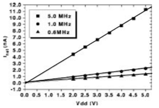
Figure 5.Inet Plotted as a function of Vdd for three frequency values. The interconnect capacitance is extracted from the slope.
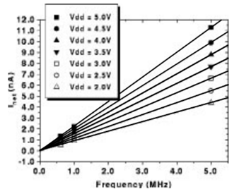
Figure 6. Inet Plotted as a function of frequency for seven Vdd values. Capacitance extracted from the slope.
| Slope Data Used for Extraction | Extracted Capacitance (fF) |
| Inet vs Vdd Frequency=5.0MHz | 0.4523 |
| Inet vs Vdd Frequency=1.0MHz | 0.4407 |
| Inet vs Vdd Frequency=0.6MHz | 0.4412 |
| Inet vs Frequency for Vdd =5.0MHz | 0.4535 |
| Inet vs Frequency for Vdd =4.5 V | 0.4399 |
| Inet vs Frequency for Vdd =4.0 V | 0.4399 |
| Inet vs Frequency for Vdd =3.5 V | 0.4395 |
| Inet vs Frequency for Vdd=3.0 V | 0.4425 |
| Inet vs Frequency for Vdd =2.5 V | 0.4429 |
| Inet vs Frequency for Vdd =2.0V | 0.4390 |
| Average | 0.4431 |
An average value of 0.44fF is obtained. This technique can be applied for characterizing the inter-wire capacitance between two parallel Metal 2 lines as a function of their separation distance, d = tdi - t the increase of capacitance as a function of distance, shown in Fig 7. An approximate dependence has observed.

Figure 7. Measured Metal 2 inter-wire capacitance versus separation distance, d.
The total capacitance between Metal 2 line and Silicon substrate, measured as a function of drawn width (Figure 7). Unit area as well as fringe Capacitance per unit length can easily extracted. Lastly, Figure 8 shows measured capacitances as a Function of total overlaps between Metal 1 and Metal 2. A saturating effect can be seen for the first time.
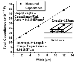
Figure 7. Measured Metal 2 capacitance over silicon substrate as a function of drawn width. Unit area and fringe capacitance per unit length can be easily demined.
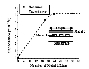
Figure 8. Measured Metal 1 to Metal 2 overlap capacitances with a constant Metal 2 length of 135µµm and Metal 1 width of 1.5µµm. The spacing between Metal 1 lines is varied. A saturating effect can be seen.
4. Methodology
Metal fills are done in hierarchical manner. Individual cells are created for each metal fill and for different shapes. These cells are then instantiated as arrays in the design depending on the requirements. Fig 9a and Fig 9b describes the same.

Fig 9 (a)
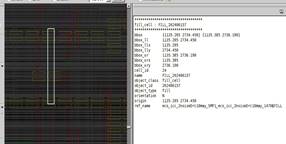
Fig 9 (b)
In PnR Tools, these arrays are created in separate database, other than the design database. While exporting the design .gds file, the two databases are merged. In addition, each time we do a change in the metal fills and re-insert metal fills, it follows different strategy and the fills are not at the same place as were in the original database. This causes uncertainty in the crosstalk impact by these fills.
That is why, when we are in the final timing closure ECO stages, after implementation of ECO we do not know how fill insertion will take place and how much it will impact the coupling capacitances of nets. Sometimes, the coupling capacitance impact on nets is huge if fill insertion does not happen properly and it gives noise issues due to metal fill capacitance. It can also affect timing of the blocks/Chips. It is also taking the large amount of time for removing and inserting the dummy fill – varying from few hours to several hours. In addition, we cannot see Dummy metal fills in the database while implementing the ECO. This can cause DRC violations with dummy metal fills such as area, spacing, via spacing violations. For removing these violations, many iterations are needed.
In this paper, we are presenting a novel methodology in which we can re-use the original Dummy metal fills and edit them to clean any new DRC violations coming because of ECO routes.
For that, we need to open our fill view of the design and through scripts, we can write out the fills of all layers with location in a file or layer by layer in several files in tcl format. Then source this file in the design database. With this method, both the design and dummy fills are visible in the same window and all the fills are editable. Shown in Fig10.

Fig.10
In this Figure, we can see the metal 3 signal routes with metal3 dummy metal fill. Any dummy fill shape of any layer can be edited to clean any DRCs/shorts with the signal routes. We can also insert metal fills layer by layer and implement the ECO manually. In addition, in this method we can create new dummy metals fills or delete any older metal fill as per our layout needs according to the metal density.
5. Benefits
There several befits of this methods are:
- Quick implementation of ECOs
- More predictable results of timing ECOs
- Less DRC violations
- Noise violations can be fixed manually.
- Effective implementation of ECOs
- Number of iteration reduced.
- Fills shapes are editable.
6. Disadvantage
There is one disadvantages in this method:
- Database size will be increased because the fills gets flattened.
7. Results
We were having 12 Noise violations: worst slack of 410volt-ps and 122 DRC violations in our example database taken for the study. ECO was created to fix these 12 noise violations and implemented through scripts.
The standard steps of ECO script is: First, it removes all kinds of fillers: Metal/Non Metal Filler cells and Dummy metal fills from database. Second step is to implement the ECO logically. Then third step is to re-route the nets, which are modified. Last step is to insert the Metal/Non-metal filler cells and Dummy metal fills and saves the database for Physical and Timing verification in Signoff.
After ECO the results degraded: 84 noise violations: worst slack of 590volt-ps mainly due to coupling capacitance between nets and Dummy metal fills. Many iterations were used to fix those noise violations but could not converge.
The new methodology was used in which the metal fills were not removed from the database. Logical ECO was implemented and routed the modified nets, and then just removed the metal fills that were causing DRCs. This iteration was final iteration and we could achieve clean results in one go.
8. Conclusion
In this paper, we have analyzed the coupling capacitance between dummy metal fills and signal metal nets and suggested a methodology to implement faster, and more predictable timing ECOs. It has less or almost zero impact on the coupling capacitance of nets and less DRCs or no DRC violations and faster convergence and closure of the design was possible.
As dummy metal fills are not required to be re-inserted in this methodology, it saves complete turn around time.
References
- B. Stine, D. Ouma, R. Divecha, D. S. Bonings, J. Chung, D. Hertherington, C. R. Harwood, O. S. Nakagawa and S.-Y. Oh. Rapid Characterization and Modeling of Pattern Dependent Variation in Chemical-Mechanical Polishing. In IEEE Trans. Semiconductor Manufacturing, volume 11, pages 129–140, 1998.
- K.-H. Lee, J.-K. Park, Y.-N. Yoon, D.-H. Jung, J.-P. Shin, Y.-K. Park and J. T Kong. Analyzing the Effects of Floating Dummy-Fills: From Feature Scale Analysis to Full-Chip RC Extraction. In IEDM Tech. Dig., pages 685–688, 2001.
- W.-S. Lee, K.-H. Lee, J.-K. Park, T.-K. Kim and Y.-K. Park. Investigation of the Capacitance Deviation due to Metal-Fills and the Effective Interconnect Geometry Modeling. In Intl. Symp. on Quality Electronic Design, page 354, 2003
- Liang, H., Kaufman, F., Sevilla, R., and Anjur, S., 1997, "Wear Phenomena in Chemical Mechanical Polishing," Wear, Vol. 211, pp. 271-279.
- A.Vittal, L. H. Chen, S. M. Marek, K.-P. Wang, and X. Yang, “Crosstalk in VLSI Interconnections,” IEEE Transactions on Computer-Aided Design of Integrated Circuits and Systems, Vol. 18, No. 12, pp. 1817-1824, December 1999.
- X. Huang, Y. Cao, D. Sylvester et al. “RLC Signal Integrity Analysis of High Global Interconnects,” IEEE International Electron Devices Meeting, pp. 731-734, Dec. 2000.
- P. Chen, D. Kirkpatrick, and K. Keutzer. Miller factor for gate-level coupling delay calculation. In Proc. ICCAD, pages 68–73, 1998.
-
J. Croix and D. Wong. Blade and razor: Cell and interconnect delay analysis. In Proc. DAC, pages 386–389, 2003.
Authors
 Sunandan Choubey
B.Tech. in Electronics and Communication Engineering from Inderprastha Engineering College, Ghaziabad.
 Himanshu Bansal
B.Tech. in Electronics and Communication Engineering from Manipal University Jaipur
 Dr. Rajendra Pratap
Ph.D. from MNNIT, Allahabad.
M.Tech and B.Tech from IIT.
Related Semiconductor IP
- NPU IP Core for Mobile
- NPU IP Core for Edge
- Specialized Video Processing NPU IP
- HYPERBUS™ Memory Controller
- AV1 Video Encoder IP
Related White Papers
- Reduce Time to Market for FPGA-Based Communication and Datacenter Applications
- Paving the way for the next generation of audio codec for True Wireless Stereo (TWS) applications - PART 5 : Cutting time to market in a safe and timely manner
- Time Interleaving of Analog to Digital Converters: Calibration Techniques, Limitations & what to look in Time Interleaved ADC IP prior to licensing
- Reduce SOC simulation and development time by designing with processors, not gates
Latest White Papers
- Ramping Up Open-Source RISC-V Cores: Assessing the Energy Efficiency of Superscalar, Out-of-Order Execution
- Transition Fixes in 3nm Multi-Voltage SoC Design
- CXL Topology-Aware and Expander-Driven Prefetching: Unlocking SSD Performance
- Breaking the Memory Bandwidth Boundary. GDDR7 IP Design Challenges & Solutions
- Automating NoC Design to Tackle Rising SoC Complexity