Memory Testing - An Insight into Algorithms and Self Repair Mechanism
By Milind Priyadarshi, eInfochips
Abstract
Typically, we see a 4X increase in memory size every 3 years to cater to the needs of new generation devices. Deep submicron devices contain a large number of memories which demands lower area and fast access time, hence, an automated test strategy for such designs is required to reduce ATE (Automatic Test Equipment) time and cost.
Memory faults behave differently than classical Stuck-At faults. Therefore, the fault models are different in memories (due to its array structure) than in the standard logic design. Also, during memory tests, apart from fault detection and localization, self-repair of faulty cells through redundant cells is also implemented.
It is also a challenge to test memories from the system level as it requires test logic to multiplex and route memory pins to external pins. To test the memories functionally or via ATPG (Automatic Test Pattern Generation) requires very large external pattern sets for acceptable test coverage due to the size and density of the cell array-and its associated faults.
Conventional DFT methods do not provide a complete solution to the requirement of testing memory faults and its self-repair capabilities. A promising solution to this dilemma is Memory BIST (Built-in Self-test) which adds test and repair circuitry to the memory itself and provides an acceptable yield. This article seeks to educate the readers on the MBIST architecture, various memory fault models, their testing through algorithms, and memory self-repair mechanism.
Introduction
Memories form a very large part of VLSI circuits. The purpose of memory systems is to store massive amounts of data.[1] Memories do not include logic gates and flip-flops. As a result, different fault models and test algorithms are required to test memories.
MBIST is a self-testing and repair mechanism which tests the memories through an effective set of algorithms to detect possibly all the faults that could be present inside a typical memory cell whether it is stuck-at (SAF), transition delay faults (TDF), coupling (CF) or neighborhood pattern sensitive faults (NPSF). It uses an inbuilt clock, address and data generators and also read/write controller logic, to generate the test patterns for the test.
Basic Memory Model

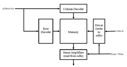
Figure 1: The Memory Model
A typical memory model consists of memory cells connected in a two-dimensional array, and hence the memory cell performance has to be analyzed in the context of the array structure. In the array structure, the memory cell is composed of two fundamental components: the ‘storage node’ and ‘select device’. The ‘select device’ component facilitates the memory cell to be addressed to read/write in an array. Scaling limits on memories are impacted by both these components.
As shown in Figure 1 above, row and address decoders determine the cell address that needs to be accessed. Based on the addresses on the row and column decoders, the corresponding row and column get selected which then get connected to sense amplifier. The sense amplifier amplifies and sends out the data.
Similarly, we can access the required cell where the data needs to be written. Special circuitry is used to write values in the cell from the data bus. For the decoders, we test the functionality whether they can access the desired cells based on the address in the address bus For the amplifier and the driver, we check if they can pass the values to and from the cells correctly.
The following fault models are sufficient for memory testing:
- Stuck-At fault
- Transition fault
- Coupling fault
- Neighborhood pattern sensitive fault (NPSF)
- Address decoder faults
MBIST Model

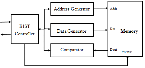
Figure 2: MBIST Model
The process of testing the fabricated chip on ATE involves the use of external test patterns applied as stimulus. The device’s response is analyzed on the tester, comparing it against the golden response which is stored as part of the test pattern data. MBIST makes this easy by placing all these functions within a test circuitry surrounding the memory on the chip itself. It implements a finite state machine (FSM) to generate stimulus and analyze the response coming out of memories.
This extra self-testing circuitry acts as the interface between the high-level system and the memory. The challenges of testing embedded memories are minimized by this interface as it facilitates controllability and observability. The FSM provides test patterns for memory testing; this greatly reduces the need for an external test pattern set for memory testing.
MBIST Algorithms
Memories are tested with special algorithms which detect the faults occurring in memories. A number of different algorithms can be used to test RAMs and ROMs. Described below are two of the most important algorithms used to test memories. These algorithms can detect multiple failures in memory with a minimum number of test steps and test time.
Checkerboard Algorithm
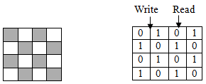
The 1s and 0s are written into alternate memory locations of the cell array in a checkerboard pattern. The algorithm divides the cells into two alternate groups such that every neighboring cell is in a different group. The checkerboard pattern is mainly used for activating failures resulting from leakage, shorts between cells, and SAF.

Figure 3: Read/Write in Checkerboard Algorithm
Algorithm Steps:
- Write checkerboard with up addressing order
- Read checkerboard with up addressing order
- Write inverse checkerboard with up addressing order
- Read inverse checkerboard with up addressing order
March algorithm
Among the different algorithms proposed to test RAMs, March tests have proved to be simpler and faster, and have emerged as the most popular ones for memory testing. There are various types of March tests with different fault coverages. A March test applies patterns that “march” up and down the memory address while writing values to and reading values from known memory locations. While retrieving proper parameters from the memory model, these algorithms also determine the size and the word length of memory.
Let’s consider one of the standard March1 algorithms which consists of 10 steps of reading and writing, in both ascending and descending address. It targets various faults like Stuck-At, Transition, Address faults, Inversion, and Idempotent coupling faults.
Algorithm Steps:
Increasing Address:
- write 0s with up addressing order (to initialize)
- Read 0s, write 1s with up addressing order
- Read 1s, write 0s with up addressing order
Decreasing address:
- Read 0s, write 1s with down addressing order
- Read 1s, write 0s with down addressing order
- Read 0s with down addressing order
Currently, most industry standards use a combination of Serial March and Checkerboard algorithms, commonly named as SMarchCKBD algorithm. This algorithm enables the MBIST controller to detect memory failures using either fast row access or fast column access.
Memory Built-in Self Repair (BISR)
Memories occupy a large area of the SoC and very often have a smaller feature size. Both of these factors indicate that memories have significant impact on yield. To avoid yield loss, redundant or spare rows and columns of storage cells are often added so that faulty cells can be redirected to redundant cells. Memory repair includes row repair, column repair or a combination of both.

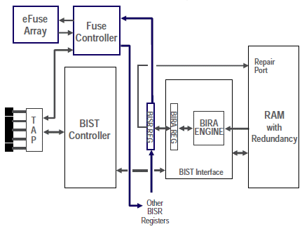
Figure 4: BISR Architecture[2]
Memory repair is implemented in two steps. The first step is to analyze the failures diagnosed by the MBIST Controller during the test for repairable memories, and the second step is to determine the repair signature to repair the memories. All the repairable memories have repair registers which hold the repair signature.
BIRA (Built-In Redundancy Analysis) module helps to calculate the repair signature based on the memory failure data and the implemented memory redundancy scheme. It also determines whether the memory is repairable in the production testing environments. The repair signature will be stored in the BIRA registers for further processing by MBIST Controllers or ATE.
The repair signature is then passed on to the repair register’s scan chain for subsequent Fusebox programming, which is located at the chip level. The reading and writing of a Fusebox is controlled through TAP (Test Access Port) and dedicated repair registers scan chains connecting memories to fuses. The repair information is then scanned out of the scan chains, compressed, and is burnt on-the-fly into the eFuse array by applying high voltage pulses.
On chip reset, the repair information from the eFuse is automatically loaded and decompressed in the repair registers, which are directly connected to the memories. This results in all memories with redundancies being repaired. Finally, BIST is run on the repaired memories which verifies the correctness of memories.
Conclusion
Research on high speed and high density memories continues to progress. In the coming years, Moore’s law will be driven by memory technologies that focus on aggressive pitch scaling and higher transistor count. Needless to say, this will drive up the complexity of testing and make it more challenging to test memories without pushing up the cost. As discussed in the article, using the MBIST model along with the algorithms and memory repair mechanisms, including BIRA and BISR, provides a low-cost but effective solution.
Author
Milind Priyadarshi
Milind Priyadarshi works as an ASIC DFT Engineer at eInfochips, an Arrow company. He has more than two years of experience in ASIC DFT, which includes working on various technology nodes, from 28nm to 7nm, handling a variety of DFT tasks.
References
-
International Technology Roadmap for Semiconductor 2.0 – ITRS
-
Memory Repair Primer – Logic Vision
Related Semiconductor IP
- NPU IP Core for Mobile
- MSP7-32 MACsec IP core for FPGA or ASIC
- UHF RFID tag IP with 3.6kBit EEPROM and -18dBm sensitivity
- NPU IP Core for Edge
- Specialized Video Processing NPU IP
Related White Papers
- Memory fault models and testing
- Testing Of Repairable Embedded Memories in SoC: Approach and Challenges
- Pie: Pooling CPU Memory for LLM Inference
- Bringing SOT-MRAM Tech Closer to Cache Memory
Latest White Papers
- Ramping Up Open-Source RISC-V Cores: Assessing the Energy Efficiency of Superscalar, Out-of-Order Execution
- Transition Fixes in 3nm Multi-Voltage SoC Design
- CXL Topology-Aware and Expander-Driven Prefetching: Unlocking SSD Performance
- Breaking the Memory Bandwidth Boundary. GDDR7 IP Design Challenges & Solutions
- Automating NoC Design to Tackle Rising SoC Complexity