Testing Of Repairable Embedded Memories in SoC: Approach and Challenges
By Charu Patel and Chintan Panchal (eInfochips)
Embedded memories play a vital role in any SoCs and almost cover more than 70% of the area in any design. These come in different sizes and types and with the shrinking of technology nodes, it becomes very crucial to test memories. Lower geometry node results into much denser memories in terms of addresses, rows and columns and as a result are more prone to defects.
Memory Built-In Self-Test (MBIST) gives the best solution to test such memories. Built in self-repair (BISR) widely used to test/repair RAM, where each RAM uses dedicated BISR circuit. The BISR feature helps to check Memory BIST logic and memory wrapper interface. Memory testing will become more effective when it adds repair features like Built-In Redundancy Analysis (BIRA) into it. Repair analysis will result into good yield of circuits. This article focuses on how to test repairable memories when we include the repair feature, and it will also look at how it will be affected during Automatic Test Pattern Generation (ATPG) or built-in pattern generation. In addition, it focuses on the common challenges and includes a comparative case study on enabling and disabling BIRA features in memories.
What is Memory Repair?
The memory repair feature diverts faulty areas of memories (e.g. row, column or both) by spare or redundant rows and columns available. Repair analysis also includes collection of faulty locations available, redundancy analysis, and analysis of how memories will access repair logic- increasing design complexity. When we are dealing with SoCs, where most of the design is covered with repairable memories, extra hardware is required to enable and disable the repair function efficiently.
Memory repair consists of different methods like row repair or column repair or both, and can be implemented as hard repair, soft repair, and fuse methods. Using a memory compiler, we can decide the number of extra rows and columns in the design. The memory design library includes the repair capacity and its characteristics.
How memory repair works: BISR and BIRA

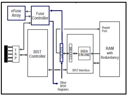
Figure 1. Built-in Self Repair (BISR) Architecture [1]
To enable repair logic for memory, the repair_analysis_present property must be enabled or turned on, which triggers repair logic in memories.
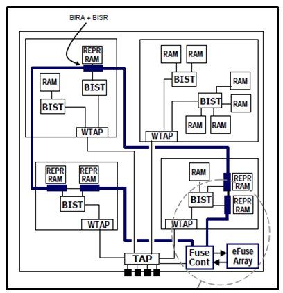
The Built-in Self Repair (BISR) logic insertion task are as follows:
- Create BISR chains in design
- Connect BISR controller to chain
- BISR controller will be connected to efuse box
- BISR controller to logic connection will be created

Figure 2. Chip BISR Architecture [2]
Challenges with repair enable
Additional Area Overhead
The primary difficulty that arises while working on repairable memory is that it will require some extra logic for repair analysis. This will affect the size and area of the chip. Having repair property enabled for memories will insert BISR and BIRA logic in design, which makes connection with controllers and efuse box. The amount of area overhead also depends on the number of repairable memories and its surrounding logic.
Dedicated BISR register modules will be inserted during MBIST insertion for repairable memories. Each type of memory has one dedicated BISR register module, which majorly includes shift registers and retiming flops. On an average each BISR register will occupy approx. 5-7% area of the total memory. Non-repairable memories, unlike BISR, have BIST area overhead of hardly 1-2%.
Scanable flops inserted for repair
Based on our experimental results we have observed that with BISR (Built in self-Repair) enabled design, the count of scanable flops in designs increases by 4-5%. Additional scan flops getting inserted in designs are categorized as mentioned in table below:
| Sr. No | MBIST Logic Insertion | Repair | Non Repair |
| 1. | Status register | √ | |
| 2. | Column/Row Fuse register | √ | |
| 3. | Spare I/O register | √ | |
| 4. | BIRA enable register | √ | |
| 5. | Error matched register | √ | |
| 6. | MBIST Retime register | √ | √ |
| 7. | BIST enable register | √ | √ |
Table 1. MBIST Logic insertion comparison
- Status register is used to check the status of repair enable/disable and repair done.
- Column and Row Fuse register is used when a particular memory is either row repairable or column repairable or both.
- Spare I/O range available register is used to check with spare row, column and input/output.
- BIRA enable register is used to check repair analysis and diagnosis done.
- Column and Row fuse registers.
- Error matched register gets enabled on detection of error, and is replaced by spare rows and columns later stage.
- BIST enable register to check whether built in self-test is enable or disable for a particular memory.
Increment in Pin Count
Unlike MBIST, repairable MBIST will cause another penalty with increased pin count at DUT/block level. During MBIST, additional pins will be required for CLK, RST, MBIST GO, and MBIST DONE. BIRA and BISR enabled circuit will include bisr_si, bisr_so, bisr_en, bisr_clk, and bisr_reset pins in design. Pins in BISR modules will majorly be dedicated pins as those will be used for repair. Nowadays, the industry uses shared pins for such logics to ensure minimum area overhead.
Higher Run Time
As there is additional logic associated with repair enable, it will insert and diagnose repair utilities through BISR logic insertion, which results in a higher run time and higher design efforts. For 1000 memories, MBIST insertion with repair enabled will take 3X higher effort and runtime compared to BISR off.
Pattern Inflation during ATPG
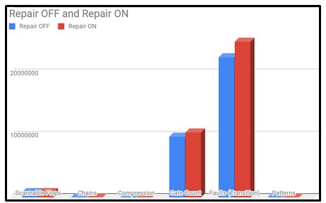
After MBIST insertion, once the design has passed through scan insertion/test logic insertion, the result is an increase in the number of scanable flip flops in design. This further results into increment in gate count, fault count and in results with more patterns during ATPG.
The below table shows comparative analysis as a case study for a design with repair on and repair off for repair analysis enabled and disabled design.
Case Study: Design A
| Design Parameters | Repair: OFF | Repair: ON | Increment in % |
| Scanable flops | 820047 | 856946 | ~4.49 |
| Chains | 1374 | 1435 | ~4.43 |
| Compression | 209 | 217 | ~3.82 |
| Gate Count | 9786679 | 10414528 | ~6.41 |
| Faults (Transition) | 22542398 | 25074024 | ~11.23% |
| Patterns | 10215 | 29627 | ~190% |
Table 2. Data Comparison for memory repair

Figure 3. Comparison Repair vs Non repair design
Conclusion
Based on what we’ve discussed so far, it can be concluded that repair analysis has its own pros and cons with positive and negative effect at the block and system/chip level. It improves manufacturing yields by repair logic, which provides the biggest cost saving factor. Lower geometry nodes always have much denser memories which are very critical to test. Today, when memory is occupying the largest area, the memory repair concept will be helpful in improving the overall manufacturing yield.
References
- [1]-[2]. ”MEMORY REPAIR PRIMER” “A Guide to Understanding Embedded Memory Repair Options and Issues”, Logic Vision.Nov.2008. Mentor graphics.
- Tessent Memory BIST User’s Manual “Implementing and verifying memory repair”, Version 2018.3. Mentor graphics.
Authors
Charu Patel
Charu Patel working as Senior Engineer in DFT BU, ASIC division, at eInfochips, an Arrow company. She has more than three years of experience in ASIC DFT, which includes working on various technology nodes, from 28nm to 7nm, handling a block and top level DFT activities.
Chintan Panchal
Chintan Panchal is working as Delivery Manager in ASIC division at eInfochips, an Arrow company. He has more than 18 years of experience in ASIC DFT. He has experience of working on various technology nodes, from 180nm to 7nm, handling different DFT tasks, and manages a team of engineers.
Related Semiconductor IP
- ReRAM NVM in DB HiTek 130nm BCD
- UFS 5.0 Host Controller IP
- PDM Receiver/PDM-to-PCM Converter
- Voltage and Temperature Sensor with integrated ADC - GlobalFoundries® 22FDX®
- 8MHz / 40MHz Pierce Oscillator - X-FAB XT018-0.18µm
Related Articles
- Internal JTAG - A cutting-edge solution for embedded instrument testing in SoC: Part 1
- Internal JTAG - A cutting-edge solution for embedded instrument testing in SoC: Part 2
- The Future of Embedded FPGAs - eFPGA: The Proof is in the Tape Out
- How Low Can You Go? Pushing the Limits of Transistors - Deep Low Voltage Enablement of Embedded Memories and Logic Libraries to Achieve Extreme Low Power
Latest Articles
- An FPGA-Based SoC Architecture with a RISC-V Controller for Energy-Efficient Temporal-Coding Spiking Neural Networks
- Enabling RISC-V Vector Code Generation in MLIR through Custom xDSL Lowerings
- A Scalable Open-Source QEC System with Sub-Microsecond Decoding-Feedback Latency
- SNAP-V: A RISC-V SoC with Configurable Neuromorphic Acceleration for Small-Scale Spiking Neural Networks
- An FPGA Implementation of Displacement Vector Search for Intra Pattern Copy in JPEG XS