High-Speed PCIe and SSD Development and Challenges
By M31 Technology
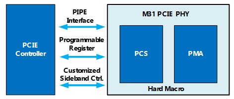
The structure diagram of PCIe and Physical Layer IP.
PCIe stands for Peripheral Component Interconnect Express (PCIe), which is a very important specification in computer buses. It is widely used in a large number of applications for data exchange communication within computer components, such as network cards, graphics cards, and nowadays NVMe solid state drives, which are mostly connected to the motherboard via PCIe. Since its introduction in 2003, PCIe has evolved into a fifth or even sixth-generation specification.
The PCIe architecture consists of a Transaction Layer, a Data Link Layer, and a Physical Layer. The Transaction Layer is the interface between PCIe and the application software, while the Physical Layer is responsible for handling the transmission of signals over the physical channel. The M31 Physical Layer IP framework (Figure 1) consists of two main components: Physical Coding Sublayer (PCS) and Physical Medium Attachment (PMA).
The PCS uses the PHY Interface for PCI Express (PIPE) interface to communicate with the PCIe controller, enabling data transfer and switching between various PCIe power modes. PMA includes analog circuits needed for external transmission, including frequency generators, transmitters, receivers, etc. M31 maintains a standardized design on the PIPE interface to improve compatibility with major PCIe controller manufacturers. On the other hand, we have also reserved some special sideband control signals to meet the needs of our customers for diverse applications. In addition, in the PMA part, as the operating speed gets higher and higher, the tolerance for channel attenuation becomes more and more demanding, from 28dB for G4 to 35dB for G5, requiring more complex equalizers to compensate. In the following paragraphs, the advantages and challenges of the various equalizers are explained.

Figure 1: M31 PCIe Physical Layer System Diagram
High-Speed Equalizer Design
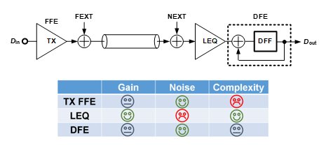
The system architecture diagram of various equalizers on the PCI transmission interface (Figure 2), includes the Feed Forward Equalization (FFE) for the transmitter, the Linear Equalizer (LEQ) for the receiver, and the Decision Feedback Equalizer (DFE) etc. Each equalizer has its own advantages and limitations and must be weighted according to the different characteristics in applications.
First, let's look at the FFE section of the diagram from the right. Although FFE reduces the signal amplitude but is particularly suitable for multi-channel interfaces as it does not amplify noise and crosstalk (FEXT, NEXT). The M31 provides full support for the 3-TAP FFE adjustment range specified by the Association, while providing fine detail control at 1/24th of the size. At the receiver end, the linear equalizer can provide the necessary voltage gain to amplify the signal to an appropriate range. It should be noted that the linear equalizer itself is prone to amplifying crosstalk and reflections, and there is a suitable bandwidth selection for different operating speeds. If a high-speed linear equalizer is used to receive data, the overall noise ratio may be reduced due to crosstalk and reflections.
It is also worth mentioning that DFE can perfectly compensate for the shortcomings of LEQ and effectively supplement the signal degradation at the Nyquist frequency without amplifying noise, which is why the association has made DFE a standard feature on receivers since PCIe G3. In addition, since the PCIe cable length is not fixed, it is important to be aware of how to automatically adjust the strength of each equalizer. Regarding this issue, M31 has optimized the three equalizers to achieve low power consumption and low area design based on the association's standard specifications. At the same time, all of the equalizer tuning algorithms have been integrated into the physical layer, effectively reducing the difficulty of IP integration for customers.

Figure 2: PCIe Equator Application Diagram
Development of PCIe in SSD
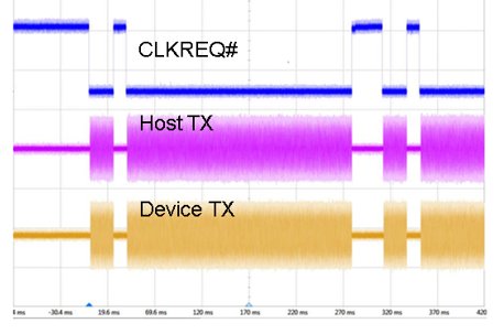
One reason for the rapid development of high-speed PCIe G4/G5 in the past two years is due to the demand for graphics and AI accelerator cards, and another important aspect is the demand for SSD hard drives. In addition to the quality of data transmission on SSD, many of the special operating modes of PCIe are becoming increasingly popular. For example, in the PCIe L1.2 power-saving mode shown in Figure 3, when CLKREQ# is pulled up, the root complex (RC) stops outputting the reference frequency, and both sides enter power-saving mode; only when there is data to be transmitted, it will immediately resume operation. As the operating speed becomes faster and the power consumption becomes higher, making power-saving functions even more important on such mobile devices. Nowadays, most of the PCIe G4 platforms on the market are already equipped with this feature, and therefore achieving low leakage and fast recovery in L1.2 has become an important part of SSD operational efficiency. M31 offers digital circuit power-off options to minimize overall leakage, while using the parameter backfill function to eliminate recalibration time. This circuit design has been tested on multiple platforms to ensure IP compatibility.
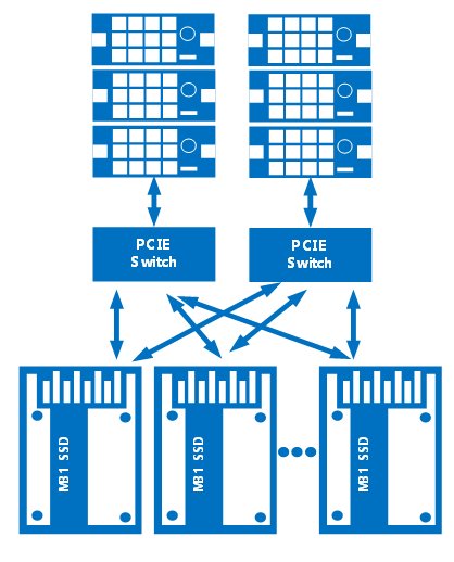
Another emerging application for PCIe is the bifurcation mode. In the past, this application was more commonly seen on the RC side, where the motherboard may have been a single X16 slot that was separated into two X8 slots by the bifurcation mode and connected to different devices. As shown in Figure 4, in the case of SSD applications, to ensure data access stability, the X4 PCIe of an SSD can be split into two X2 paths and connected to different RCs. In this way, if there is a problem with the first RC, the hard disk data can still be accessed through the second RC. If we do not need bifurcation mode, we can also connect the full X4 to the same RC to provide the highest transmission rate. In IP design, M31 provides such flexibility to support RC or EP bifurcation applications and can integrate up to one X16 IP to provide higher bandwidth.

Figure 3: L1.2 Operation Timing Diagram

Figure 4: SSD Bifurcation Application
M31 Professional PCIe Technical Service
M31's professional technical team has been working in the PCIe field for ten years, covering technology nodes ranging from 7nm to 55nm, and has a complete layout for different needs, with customers ranging from SSD storage chip companies, home audio/video network chip companies to graphics card chip design companies. The M31 technical team not only focuses on IP development, but also provides a full range of technical support services, and has built up complete measurement equipment, from signal quality analysis, and electrical characteristics measurement to system compatibility testing, working closely with customers to provide chip design optimization solutions for product applications, thus enhancing customers' product competitiveness.
Related Semiconductor IP
- AXI Bridge with DMA for PCIe IP Core
- PCIe Gen 7 Verification IP
- PCIe Gen 6 Phy
- PCIe Gen 6 controller IP
- PCIe GEN6 PHY IP
Related White Papers
- PCIe 5.0: The universal high-speed interconnect for High Bandwidth and Low Latency Applications Design Challenges & Solutions
- Conquering the challenges of PCIe with NVMe in order to deliver highly competitive Enterprise PCIe SSD
- Understanding Logic Equivalence Check (LEC) Flow and Its Challenges and Proposed Solution
- Emerging Trends and Challenges in Embedded System Design
Latest White Papers
- On the Thermal Vulnerability of 3D-Stacked High-Bandwidth Memory Architectures
- OmniSim: Simulating Hardware with C Speed and RTL Accuracy for High-Level Synthesis Designs
- Balancing Power and Performance With Task Dependencies in Multi-Core Systems
- LLM Inference with Codebook-based Q4X Quantization using the Llama.cpp Framework on RISC-V Vector CPUs
- PCIe 5.0: The universal high-speed interconnect for High Bandwidth and Low Latency Applications Design Challenges & Solutions