Generic DDR Behavioural Model
HaribhaiSomabhai Patel, AmarkumarKiritbhai Solanki (eInfochips)
Abstract
SOC (System On Chip) and behavioural designs are integrating more systems and functions to meet market demands for improved user experience. More often than not, these systems and functions require access to off-chip DRAM to support the required increase in compute performance. As not all of the systems access DRAM in the same fashion, with the same traffic pattern, or with the same bandwidth requirement, designers must find the right technique to efficiently balance off-chip DRAM access for all of the behavioural designs.
This paper represents a generic executable architecture. It represents the efficient behaviour of the Memory Model to be used for verification of SOC communicating with DDR SDRAMs or can be used as the third party Model verification (passive element). Paper shows the capability as standalone VIP architecture and also represents the market value of DDR model in the present technical era with different technical views and challenges faced. It also givessolution of supporting different part number of established DDR vendors like Micron, Elpida, Samsung etc.
Introduction:
Access to off-chip DDR SDRAM has been an integral part of behavioural design for many years. When considering DDR interface IP, designers have a choice of whether to make the IP themselves or to license it from a third-party IP provider. In making this choice, they need to consider many business-related as well as technical factors. For discussion purposes, this article will focus on the technical criteria for making DDR interface IP with an ease.
As like with most Behavioural Models, criteria for selecting DDR interface IP includes features and performance. As more features and applications are integrated into IPs, the required processing power of the CPU and other processing functions must increase as well. The increase in processing power typically goes hand-in-hand with the increase in DDR bandwidth requirements, thus making performance the most important criteria in DDR IP selection. As an increase in frequency is the most common contributor to an increase in performance, performance is often thought of in terms of MHz. However, with a DDR SDRAM subsystem, increasing performance involves a lot more than simply increasing frequency.
DDR stands for “Double Data Rate”. In older SDRAM technology DATA bits were sampled or supplied only at the single edge (positive edge) of the clock. With the newer DDR technology the data bits are sampled or supplied at both the edges (positive and negative edge) of the clock and therefore the throughput per clock is doubled every single clock cycle. DDR involves the complex protocol logic with accurate timings. As the technology progresses, the DDR also gets updated with the modified protocol logic.
Types of DDRs available In the Market:
- DDR: Double Data rate
- DDR
- DDR2
- DDR3
- DDR4
- LPDDR: Low Power Double Data Rate
- LPDDR
- LPDDR2
- LPDDR3
- GDDR : Graphics Double Data Rate
- GDDR
- GDDR2
- GDDR3
- GDDR4
- GDDR5
Originally, DDR SDRAM was architected with one primary purpose, which manifested into the DDR SDRAM architecture we are familiar with today. The primary purpose was to create an off-chip memory that was also low cost in terms of size and pin count. SDRAM memory cells are very small and constructed of a single pass gate transistor and capacitor to store the charge.
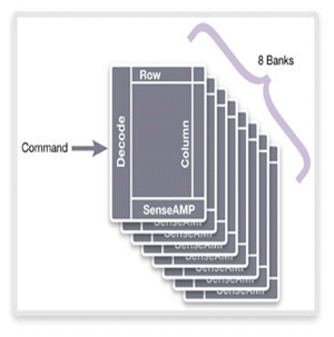
DDR2 SDRAM chips contain multiple independent memory banks--typically eight banks, as shown in Figure 1. A bank is idle, active, or changing from one to the other. An “activate” command “opens” an idle bank and reads the specified row data into an array of sense amplifiers where the data is stored during all read and write operations.

Figure 1 : DRAM with 8 banks
The Read or Write access to any row is started with an active transaction. User needs to open a row with a given bank and row address, generally known as activating the row. Then they need to send the bank address and column address to send read or write transactions.
When the memory controller wants to access a different row, it must first return that bank's sense amplifiers to an idle state, ready to sense the next row. This is known as a "pre-charge" command, or "closing" the row. There is a minimum time that must transpire while the bank becomes fully idle and it can receive another activate command.
Among all types of the DDR and LPDDR memories, the protocol differs with slight modifications. If we see the interface of the current DDRs (DDR2 and DDR3), that remains the same. Thedifference between all types of DDRs is limited to the minor level of functionality which can be taken care using System-Verilogclasses’ implementation.
Generic DDR Model Architecture
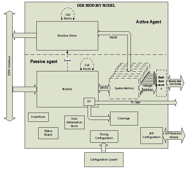
Figure 2 : Architecture diagram
Monitor:
Monitor constantly monitors the interface of the DDR. Convert pin level data to abstract high level transaction which will be communicated to different blocks.Monitor implements complex FSM of DDR. It triggers the reactive driver on detection ofany transaction where driver has to response to controller. Whenever the WRITE command is detected the data will be sampled from data interface and written into sparse memory based on Bank, Row and Column address. Monitor will also implement all the checkers which will be triggered and shout in case of any wrong behaviour from controller.
Driver:
The Driver will be reactive in nature; it is mostly responsible for driving the response. Driver will be waiting for an event from the Monitor to start driving. The event from the monitor gets triggered when the any transaction is detected where Model has to send response back to the controller. As soon as the event from the monitor gets triggered, the driver starts collecting the status of the state machine and status object. Based on the state, driver collects the addresses. With provided bank, row and column it collects data from Memory and puts it back on the DDR interface.
Auto Initialization:
Initialization process involved with DDR protocol is long and consumes a valuable time. But initialization will not be required to validate all the types of scenario. An auto initialization option we can provide, which can save valueable simulation time.
MR Configuration:
The functionality of the DDR depends on its Mode Registers configured by the user. It will be updated bsed on MRW operation and read during MRR operation of DDR. Backdoor access we can provide to the user as DDR has may read only field, which will be configured at the time of manufaturing of DRAM. Backdoor also helps for reading values of write only fields.
Back Door:
Now days with the complex protocols it becomes time consuming to configure the systems with following the protocol. So to save the precious timings back door is the correct solution. The presented architecture provides that facility from which the user is able to configure the Mode Registers and so the functionality of the Model. Also the back door access of the Sparse Memory is given to the user. User can comfortably write the data to the memory which saves the precious and lengthy simulation time. User also can read the data from memory through backdoor in order to verify write transaction correctness.
Analysis Port (AP):
Analysis port is a well-defined mechanism which can serve the purpose of verifying the response of active and passive elements at higher level of SOC designs. If we consider a case where the DDR is mounted as a secondary device at higher level of SOC,where user is interested in collecting sampled transaction from DDR interface. This analysis port can be connected to the one port of the scoreboard which will give actual data and user can connect other port of the scoreboard with their expected data which can be coming from PCI express/other component of the SOC which will write/read data to/from the DDR DRAMs.
Call backs:
Architecture shows important implementation of driver call backs. Today with current technology era, we have such importance with call backs. The most important application of the call back is the erroneous testing for the Model. How the Modelresponds with the erroneous scenarios and capability of Model in injecting the error.
This implementation is done with taking the transaction instance with the driver call back method. We can get the generated transaction through the call backs and then can change the behaviour of a particular transaction. This change we can make on the transaction where we want and thus we can verify the functionalities of Model as well as behaviour of controller also.
Call-backs can be implemented at the various stages of the transaction like, at the start of transaction, at the start of address phase, at the start of data phase, at the end of transaction etc.
Timing Configuration Loader:
Timings are the most important configuration parameters with DDR protocol. Each Model supporting particular frequency band will have timing ranges according to JEDEC standards. Each memory vendor will have Memory Model with different part numbers. These part numbers are based on the frequency that they are supporting and the Memory capacity configuration. To make the model generic it can be a major challenge to configure each part number with its own timing parameter values.To resolve this challenge we can have the timing configuration loader,which will load the timings based on the configuration selected and the frequency support.
Configuration file for all the available part number can be created, which will be loaded through configuration loader. This can be done using some script which will select part number of user choice and load it into the memory model.Scripts have to serve multi purposes here. Scripts should be capable to give flexibility to user that they can choose the vendors and the configurations for the part numbers they want. Such freedom of choosing the parameters will give the ease to user to generate the Model based on his needs.
Customize option can also be provided to user to have an immense of facility that user can change few paramneters of a part number according to his need. Considering a case where user wants to run the part number which is working on 533 Mhz and so clock period is 1.876 to 532 MHz. This customize option will help the user to change the clock period when generating the model. So he can edit the clock period and make it 1.879. We can consider such cases where this customize option can serve the capability to the GUI which can generate the model according to the users configurations. Moving aheadwith customizeoptionwe can still provide the user facility toload an existing model and then change the parameters but the parameters should be based on the standards.
Applications
The most usual application for the DDR Memory is presented with a snap below. This case represents the slave behaviour of DDR memory. The DDR memory model has given a tremendous performance with the existing processor and with the existing cutting edge technologies. The higher speed and the efficiency have challenged the technical world to have more precious memory compared with the existing one. The DRAM is connected at SOC level shows the complexity of the systems and the importance of the Model from the application point of view.

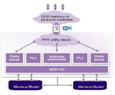
Figure 3: Use case of memory model.
Use case of Memory Model
The DDR model implementation gives many use cases and ways to connect the model efficiently. The model becomes very useful in verifying of the SOC which will have the DDR controller. As shown in above figure 3, Memory Model can be connectedto DDR interface for the verification of the SOC communicating with DDR memories. Model will behave as DDR DRAM and also provide additional advance features like inbuilt checkers, functional coverage, analysis port to collect sampled transaction, backdoor access to memory, Error injection, call back execution at different level of transaction etc. All this advance features will help user a lot for the verification of the SOC.
Using as a passive component
Presented memory model can also be used as passive component to verify the third party DDR memory model connected with the DDR interface. Connecting it as a passive element it will just avoid sending response to the DRAM controller but it provides all the advance features like checkers, functional coverage etc. as listed above.
Related Semiconductor IP
- NPU IP Core for Mobile
- NPU IP Core for Edge
- Specialized Video Processing NPU IP
- HYPERBUS™ Memory Controller
- AV1 Video Encoder IP
Related White Papers
- Generic Driver Model using hardware abstraction and standard APIs
- Behavioral Model of a DDR Memory Controller in a DFi - Frequency Ratio System
- Reuse of system-level model key
- Fabless ASIC model debated
Latest White Papers
- Ramping Up Open-Source RISC-V Cores: Assessing the Energy Efficiency of Superscalar, Out-of-Order Execution
- Transition Fixes in 3nm Multi-Voltage SoC Design
- CXL Topology-Aware and Expander-Driven Prefetching: Unlocking SSD Performance
- Breaking the Memory Bandwidth Boundary. GDDR7 IP Design Challenges & Solutions
- Automating NoC Design to Tackle Rising SoC Complexity
