Behavioral Model of a DDR Memory Controller in a DFi - Frequency Ratio System
Supriya Upadhya , Nithin Kumar (Mindtree Ltd)
Abstract
The design of a Memory Controller (MC) and its integration to a system has long posed difficult challenges to engineers and system architects. Interoperability between a Memory Controller and a PHY is one such challenge. DFi™ is a standard that ensures the compatibility of DDR MC and DDR PHY at target matched frequencies and frequency ratios.
In a frequency ratio system, the MC operates at half rate or quarter rate of the PHY frequency. Hence, the timing relationship between DFi™ signals can only be expressed in 2x or 4x of the PHY clock for a non-phased operation. For phased operation, dedicated buses allow the establishment of timing relationship other than 2x or 4x PHY clocks.
The phase information is encoded by the MC and issued as the ‘Phase N’ signals. The PHY decodes the ‘Phase N’ signals to generate the required timing signal and uses it for further operation.
The DFi™ specification does not specify any format for phase encoding and exchange. This is left to the implementation. This paper presents a phase encoding algorithm for the MC to establish a desired timing relationship with PHY in a DFi™ frequency ratio system. The distinction of this approach is that the entire implementation of the phase relationship between MC and PHY is reduced to a simple mathematical equation.
INTRODUCTION
The paper details the DDR MC Phase encoding algorithm in a DFi™ frequency ratio system. It is intended for a technical audience interested in learning about how the DDR MC encodes the PHY timing information in the Phase- Specific bus. Please refer to the DFi™ 3.1 specification for complete details on frequency ratio systems.
DFi™ is pervasive industry specification that defines an interface protocol between DDR memory controllers and PHYs [2]. It enables the development of systems-on-chip (SoCs) that support the latest DRAM standards.[1] Understanding the DFi™ from a MC perspective across all frequency-ratio systems can simplify the developments of the verification components for the the protocol.
In DFi™ frequency-ratio system, Phasing is an important concept that helps the DDR-MC to communicate timing parameters to the DDR-PHY. However, DDR MC Phase encoding algorithm for a frequency ratio system is not in the specification. Although, this algorithm is implementation specific, knowledge of the MC phase encoding algorithm is important to effectively understand the control structure of the MC.
Existing algorithms for phase encoding are design implementation specific and hence rarely exposed. As a Design Verification Engineer, you may look up to the approach explained in this paper to verify the phase encoding feature of the DFi™ compliant DDR-MC. This algorithm significantly improves an engineer’s productivity in developing verification components.
The key component of this approach is the generalization of mechanism in which the two different systems function. The sections to follow detail the below mentioned aspects.
- Frequency Ratio Across the DFI
- Frequency Ratio Clock Definition
- Write and Read Data Interface in Frequency Ratio Systems
- Encoding Timing Relationship Parameters
- Conclusions and Related work.
THE BODY
A. Frequency Ratio Across the DFi [2]
The DFI is defined at the MC to PHY boundary and therefore operates in the clock frequency domain of the MC. The MC clock is always the DFI clock and all DFI signals are referenced from the MC clock. In a DDR memory subsystem, it may be advantageous to operate the PHY at a higher frequency than the MC. If the PHY operates at a multiple of the MC frequency, the PHY transfers data at a higher data rate relative to the DFI clock and the MC has the option to execute multiple commands in a single DFI clock cycle.
The DFI specification supports a 1:2 or 1:4 MC to PHY frequency ratio, defining the relationship of the reference clocks for the MC and the PHY.
DFI signals may be sent or received on the DFI PHY clock, provided the signals reference the rising edge of the DFI clock and the clock is phase aligned. The MC communicates frequency ratio settings to the PHY on the dfi_freq_ratio signal. This signal is only required for devices using this frequency ratio protocol.
B. Frequency Ratio Clock Definition[2]
The DFI clock and the DFI PHY clock must be phase-aligned and at a 1:2 or 1:4 frequency ratio relative to one another. Some DFI signals from the MC to the PHY must communicate information about the signal in reference to the DFI PHY clock to maintain the correct timing information. Therefore, the DFI PHY clock is described in terms of phases, where the number of clock phases for a system is the ratio of the DFI PHY clock to the DFI clock.

Fig. 1 Frequency Ratio 1:2 Phase Definition
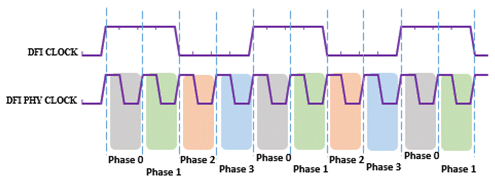
Fig. 2 Frequency Ratio 1:4 Phase Definition
C. Interface Signals with Frequency Ratio Systems [2]
Write data and read data signals are defined on a per-phase basis and all signal timing is in reference to the DFI clock. The PHY must account for any assertions based on the DFI clock. Any signals driven by the PHY must only change during phase 0 of the DFI PHY clock to allow the MC the full DFI clock to capture the signal change.
The DFI specification supports the ability to send a unique command on each phase of the DFI PHY clock. To communicate this information to the PHY, the DFI specification defines commands for a frequency ratio system in a vectored format. The PHY must maintain this information to preserve the timing relationships between commands and data. Therefore, for frequency ratio systems, the control signal interface, the write data interface and the read data enable signal are all suffixed with a “_pN” where N is the phase number. As an example, for a 1:2 frequency ratio system, instead of a single dfi_address signal, there are 2 signals: dfi_address_p0 and dfi_address_p1. The read data signal, read data valid and read data not valid signals are suffixed with a “_wN” where N is the DFI data word.
D. Write Data Interface in Frequency Ratio Systems[2]
The write data enable signal (dfi_wrdata_en_pN) indicates to the PHY that valid dfi_wrdata will be transmitted in Tphy_wrdata cycles and its width defines the number of data phases of the write. In order to communicate this information to the PHY, the phase information must be encoded within the signal. Therefore, this signal is also vectored into multiple signals based on the frequency ratio. Similar to the DFI command, each signal is associated with a phase of the DFI PHY clock.
E. Read Data Interface in Frequency Ratio Systems[2]
Similar to the write data enable signal, the read data enable signal (dfi_rddata_en_pN) defines the number of clocks between the read command and the read data, and its width defines the number of data phases of the read. The PHY sends read data to the MC on the dfi_rddata_wN buses whenever read data is available, asserting the associated dfi_rddata_valid_wN signals to inform the MC which buses contain valid data. Unlike the read data enable signal which correlates to the phase of the DFI PHY clock, the read data, read data valid and read data not valid signals are all vectored with the DFI data word suffix.
F. Encoding Timing Relationship Parameters
Since the max number of phases in a 1:2 frequency ratio system is 2 , we can represent ‘phase N’ in base 2 number system (phase 0 and phase 1) . Similarly the max number of phases in a 1:4 frequency ratio system is 4 . Hence , we can represent ’phase N’ in base 4 number system (phase 0 , phase 1 , phase 2 , phase 3) . This takes care of the rotational order rule that the DFI specifies.
i.e.,
a) If command is being driven on Phase 0, then N = 0 and N+1 = 1 and ((N+1) +1) = 0 and so on.
b) If command is being driven on Phase 1, then N = 1 and N+1 = 0 and ((N+1) +1) = 1 and so on.
Table 1: Remainders for frequency ratio systems
| Frequency Ratio | Remainder (R1) | Remainder(R2) |
| 1:2 | mod (Tphy_wrlat /2) | mod (Tphy_wrdata, 2) |
| 1:4 | mod (Tphy_wrlat /4) | mod (Tphy_wrdata, 4) |
Table 2: Quotients for frequency ratio systems
| Frequency Ratio | Quotient(Q1) | Quotient(Q2) |
| 1:2 | floor(Tphy_wrlat /2) | floor(Tphy_wrdata /2) |
| 1:4 | floor(Tphy_wrlat /4) | floor(Tphy_wrdata /4) |
In Table 1, R1 and R2 indicate the remainders when the PHY latency is divided by 2 and 4 in a 1:2 and 1:4 frequency ratio system respectively.
In Table 2, Q1 and Q2 indicate the quotients when the PHY latency is divided by 2 and 4 in a 1:2 and 1:4 frequency ratio system respectively.
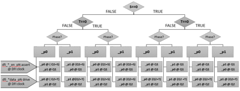
(R1! =0)? (S=1) :( S=0) (1)
(R2! =0)? (T=1) :( T=0) (2)
From equations “(1)” and “(2)” , S indicates the divisiblity of Tphy_wrlat by 2 and 4 in a 1:2 and 1:4 frequency ratio system respectively. R indicates the divisibility of Tphy_wrdata by 2 and 4 in a 1:2 and 1:4 frequency ratio system respectively.
G. Encoding Timing Relationship Flowchart
Fig. 3 represents the phase encoding algorithm for a 1:2 frequency ratio system. It explains how the dfi_wrdata_en_pN and dfi_rddata_en_pN signals are asserted based on the latency supported by the PHY for commands arriving on various phase. It also explains how the timing relationship between various data words is encoded within the phase specific data bus adhering to the rotational order rule.
Table 3 shows the DFI clock at which the enable is asserted after the command is issued in a phase specific bus .
Table 3: Timing relationship for enable signals
| S | T | T_en |
| 0 | 0 | Q1 |
| 0 | 1 | Q1 |
| 1 | 0 | Q1+S |
| 1 | 1 | Q1+S |
Table 4 shows the DFI clock at which the data words are driven after the enable is asserted in a phase specific bus based on the values of S and T .
Table 4: Timing relationship for data words
| S | T | T_data |
| 0 | 0 | Q2+T |
| 0 | 1 | Q2+T |
| 1 | 0 | Q2+¯T |
| 1 | 1 | Q2+T |
From Table 3 we have ,
T_en = Q1+S (3)
From Table 4 we have ,
T_data = Q2+¯S T+S (4)
Fig. 3 Phase encoding algorithm flowchart for 1:2 frequency ratio system
From equations “(3)” and “(4)” we can establish a timing relaionship between the enable and data signals.
Table 5 shows the mathematical deduction for MC encoding algorithm for a 1:2 frequency ratio system. _pN indicates the phase specific bus in which the command is driven .
Table 6 shows the result generalized for a 1:4 and 1:2 frequency ratio system by incorporating “(R1-S)” and “(R2-T)” factors. These factors do not impact the phase encoding in the 1:2 frequency domain .
Table 5: MC Encoding for a 1:2 frequency ratio system
| dfi_wrdata_en/dfi_rddata_en | dfi_wrdata/dfi_rddata_valid/dfi_rddata |
| _pN asserted @T_en DFi clock cycles after command. | _pN to _p[N+S*T] asserted @T_data DFi clock cycles from assertion of the first enable. |
| Remaining _pN asserted @Q1 DFi clock cycles after command. | Remaining _pN (if any) asserted @ Q2 after assertion of first enable. |
Table 6: MC Encoding for all frequency ratio system
| dfi_wrdata_en/dfi_rddata_en | dfi_wrdata/dfi_rddata_valid/dfi_rddata |
| _pN to _p[N+(R1 - S)] asserted @T_en DFi clock cycles after command. | _pN to _p[N+(R2-T)+S*T] asserted @T_data DFi clock cycles from assertion of the first enable. |
| Remaining _pN asserted @Q1 DFi clock cycles after command. | Remaining _pN (if any) asserted @Q2 DFi after assertion of first enable. |
Table 7 shows the minimum number of DFI clocks for which the dfi_*_en_pN must be asserted for various burst lengths on the DDR-MC side.
Table 7: High time for enable signals for various burst lengths
| Frequency Ratio | BL2 | BL4 | BL8 | BL16 |
| 1:1 | 1 | 2 | 4 | 8 |
| 1:2 | - | 1 | 2 | 4 |
| 1:4 | - | - | 1 | 2 |
III EXAMPLES
The following examples explain the various combination of PHY latencies and the MC phase encoding algorithm for these latency.
a. Tphy_wrlat = 2; Tphy_wrdata = 2
Fig. 4 shows a 1:2 Frequency ratio Single Write command with data word of burst length 16
Assume Tphy_wrlat = 2; Tphy_wrdata = 2 and MC intends to transmit a data word of burst length 16 . Let us assume that the WRITE command is issued in Phase 0 of the DFI command bus .
Since Tphy_wrlat is divisible by 2 , parameter S(equals 0) has no effect on the encoding of the dfi_wrdata_en_pN . The MC asserts the dfi_wrdata_en_p0 and dfi_wrdata_en_p1 at Q1 DFI clocks following the WRITE command .
Since Tphy_wrdata is divisible by 2 ,parameter S(equals 0) and T(equals 0) have no effect on the encoding of the dfi_wrdata_pN . The first data word (D0) and next data word (D1) is driven in dfi_wrdata_p0 and dfi_wrdata_p1 respectively after Q2 DFI clock cycles from the assertion of dfi_wrdata_en_p0 . The subsequent data words (D2, D3, D4, D5, D6, and D7) are driven incrementally in the subsequent phases (p0, p1, p0... etc.) in the following clock edges.
b. Tphy_wrlat = 2; Tphy_wrdata = 1
Fig. 5 shows a 1:2 Frequency ratio Single Write command with data word of burst length 16 ..
Assume Tphy_wrlat = 2; Tphy_wrdata = 1 and MC intends to transmit a data word of burst length 16 . Let us assume that the WRITE command is issued in Phase 0 of the DFI command bus .
Since Tphy_wrlat is divisible by 2 , parameter S(equals 0) has no effect on the encoding of the dfi_wrdata_en_pN . The MC asserts the dfi_wrdata_en_p0 and dfi_wrdata_en_p1 at Q1 DFI clocks following the WRITE command
Since Tphy_wrlat is divisible by 2 and Tphy_wrdata is not divisible by 2 , Tphy_wrdata encoding is affected by parameter T(equals 1) only . MC drives the first data word(D0) in dfi_wrdata_p1 bus at Q2 DFI clock after the first dfi_wrdata_en_pN is asserted and the next data word(D1) in the dfi_wrdata_p0 bus at (Q2+T) DFI clock after the first dfi_wrdata_en_pN is asserted. The subsequent data words (D2, D3, D4, D5, D6, and D7) are driven incrementally in the subsequent phases (p0, p1, p0... etc.) in the following clock edges.
c. Tphy_wrlat = 3; Tphy_wrdata = 2
Fig. 6 shows a 1:2 Frequency ration Single Write command with data word of burst length 16
Assume the Tphy_wrlat = 3; Tphy_wrdata = 2 and MC intends to transmit a data word of burst length 16 . Let us assume that the WRITE command is issued in Phase 0 of the DFI command bus .
Since Tphy_wrlat is not divisible by 2 , parameter S (equals 1) has certain effect on the encoding of the dfi_wrdata_en_pN . The MC asserts the dfi_wrdata_en_p1 at Q1 DFI clock and dfi_wrdata_en_p0 at (Q1+S) DFI clocks following the WRITE command .
Since Tphy_wrlat is not divisible by 2 and Tphy_wrdata is divisible by 2 , Tphy_wrdata encoding is affected only by parameter S . MC drives the first data word(D0) in dfi_wrdata_p1 bus at Q2 DFI clocks after the first dfi_wrdata_en_pN is asserted and the next data word (D1) in the dfi_wrdata_p0 bus at (Q2+S) DFI clocks after the first dfi_wrdata_en_pN is asserted. The subsequent data words (D2, D3, D4, D5, D6, and D7) are placed incrementally in the subsequent phases in the following clock edges.
d. Tphy_wrlat = 3; Tphy_wrdata = 3
Fig. 7 shows a 1:2 Frequency ration Single Write command with data word of burst length 16 .
Assume the Tphy_wrlat = 3; Tphy_wrdata = 3 and MC intends to transmit a data word of burst length 16 . Let us assume that the WRITE command is issued in Phase 0 of the DFI command bus .
Since Tphy_wrlat is not divisible by 2 , parameter S ( equals 1) has certain effect on the encoding of the dfi_wrdata_en_pN . The MC asserts the dfi_wrdata_en_p1 at Q1 DFI clock and dfi_wrdata_en_p0 at (Q1+S) DFI clocks following the WRITE command .
Since Tphy_wrlat is not divisible by 2 and Tphy_wrdata is also not divisible by 2 , Tphy_wrdata encoding is affected by both parameter S(equals 1) and parameter T(equals 1) . MC drives the first data word(D0) and the second data word(D1) in dfi_wrdata_p0 bus and dfi_wrdata_p1 bus respectively at (Q2+S) DFI clocks after the first dfi_wrdata_en_pN is asserted . The subsequent data words (D2, D3, D4, D5, D6, and D7) are placed incrementally in the subsequent phases in the following clock edges.
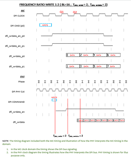
Fig.4 1:2 Frequency Ratio Single Read with even Tphy_wrlat and even Tphy_wrdata
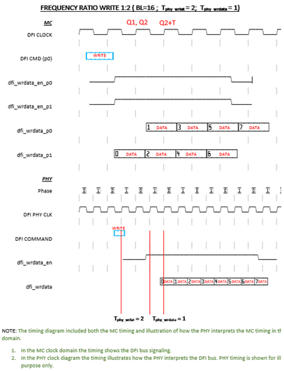
Fig.5 1:2 Frequency Ratio Single Read with even Tphy_wrlat and odd Tphy_wrdata
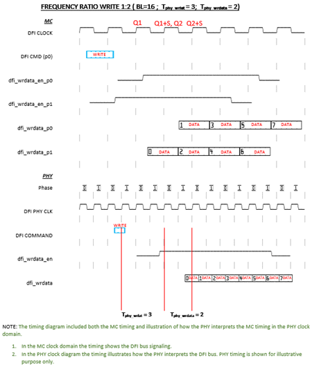
Fig.6 1:2 Frequency Ratio Single Read with odd Tphy_wrlat and even Tphy_wrdata
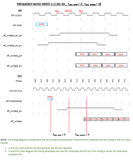
Fig.7 1:2 Frequency Ratio Single Read with odd Tphy_wrlat and odd Tphy_wrdata
IV. LIMITATIONS
This algorithm cannot be applied to a system that does not fall in the category shown in Table 8. Many DFI systems do not require support for burst transfers that are not a multiple of the frequency ratio. For example, with a 4:1 frequency system, a burst of 4 DRAM words of data is transferred on 2 DFI data words.
However, if a system does support these burst transfers, the PHY must transfer the read data in a rotational order. Creating a system supporting this combination, i.e., when the DFI read data for a single read does not use the entire DFI read data interface, involves additional complexity that needs to be accounted.
| Frequency Ratio | BL2 | BL4 | BL8 | BL16 |
| 1:1 | Yes | Yes | Yes | Yes |
| 1:2 | - | Yes | Yes | Yes |
| 1:4 | - | - | Yes | Yes |
Table 8: Recommendations for Encoding Algorithm
CONCLUSIONS
We proposed a behavioral model phase encoding algorithm in a DFI compliant DDR-Memory controller. This algorithm can be used to model the DDR-MC in RTL. This algorithm is proven helpful in from scratch development of various ASIC verification components such as driver, monitor and scoreboard in a DFi verification environment and thereby reducing the verification efforts.
FUTURE WORK
We are currently extending the algorithm to 1:2N (N>2) frequency ratio, and preliminary results are encouraging. Although there is no discussion regarding a frequency ratio greater that 1:4. The algorithm can be extended to a future memory type supporting higher frequency ratios.
ACKNOWLEDGEMENTS
The authors would like to thank Santosh Shivadatta (Director & Head – VLSI ,Engineering R&D Service Line , Mindtree Ltd) and Kumar S ( Project Manager , VLSI ,Engineering R&D Service Line , Mindtree Ltd) for their valuable comments and suggestions to improve the quality of the paper. They are also grateful to Vinod Vishwa Gadde ( Senior Engineer , Mindtree Ltd) for content review of this paper . The paper benifited greately from comments by John MacLaren (Committee Chair, DFi) . This work was supported in part by Mindtree VLSI-CoE.
REFERENCES
[2] DFi™ Specification document
[3] Eilam, Eldad & Chikofsky, Elliot J. (2007). Reversing: secrets of reverse engineering. John Wiley & Sons. p. 3. ISBN 978-0-7645-7481-8.
ABOUT THE AUTHORS
 Supriya Upadhya received B.E degree in Electronics and Communication Engineering from MS college of Engineering Bangalore, India in 2010. Currently she is working as senior Engineer at eRnD VLSI service line in Mindtree Ltd Bangalore. Her expertise area includes ASIC , SOC verification amd post silicon validation.
 Nithin V R Kumar received B.E degree in Electronics and Communication Engineering from JSS Academy of Technical Education Bangalore, India in 2011. Currently he is working as Senior Engineer at eRnD VLSI service line in Mindtree Ltd Bangalore. He has expertise in IP level verification.
Related Semiconductor IP
- ReRAM NVM in DB HiTek 130nm BCD
- UFS 5.0 Host Controller IP
- PDM Receiver/PDM-to-PCM Converter
- Voltage and Temperature Sensor with integrated ADC - GlobalFoundries® 22FDX®
- 8MHz / 40MHz Pierce Oscillator - X-FAB XT018-0.18µm
Related Articles
- Fault Injection in On-Chip Interconnects: A Comparative Study of Wishbone, AXI-Lite, and AXI
- A Direct Memory Access Controller (DMAC) for Irregular Data Transfers on RISC-V Linux Systems
- Creating a Frequency Plan for a System using a PLL
- Paving the way for the next generation of audio codec for True Wireless Stereo (TWS) applications - PART 5 : Cutting time to market in a safe and timely manner
Latest Articles
- An FPGA-Based SoC Architecture with a RISC-V Controller for Energy-Efficient Temporal-Coding Spiking Neural Networks
- Enabling RISC-V Vector Code Generation in MLIR through Custom xDSL Lowerings
- A Scalable Open-Source QEC System with Sub-Microsecond Decoding-Feedback Latency
- SNAP-V: A RISC-V SoC with Configurable Neuromorphic Acceleration for Small-Scale Spiking Neural Networks
- An FPGA Implementation of Displacement Vector Search for Intra Pattern Copy in JPEG XS
