A configurable FPGA-based multi-channel high-definition Video Processing Platform
Abstract :
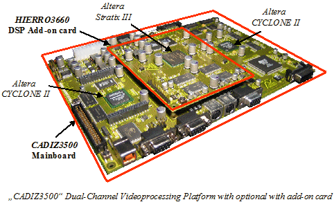
The following paper describes an FPGA-based high-definition video processing platform. The platform supports a wide range of applications including flat-panel TV, projection TV and video monitor. The paper and the presentation focus on the platform concept, the signal processing capabilities and the display controller applications. The display controllers are designed for the industrial, information, professional video, consumer and medical display markets. All major signal processing tasks are FPGA based allowing maximum flexibility and quick turnaround times. The platform consists of a video processing mainboard (CADIZ3500), an optional DSP add-on card (i.e. HIERRO3660), IP design packages, and software packages. This approach provides the most flexibility in developing customized applications, and in meeting cost and performance requirements. The platform can decode, process and overlay multiple PC graphic/On-Screen Display (OSD), High-Definition (HD) and Standard-Definition (SD) video inputs simultaneously. Resulting images can be displayed directly on LCD or PDP flat-panel displays. In addition to flat-panel interfacing, the standard computer monitor interface allows simultaneous display of the same content or a different content on a second display.
Platform features:
- Flexible FPGA based signal processing
- HDTV: 720p, 1080i, 1080p 50/60 Hz
- SDTV: 480i/p and 576i/p 50/60Hz
- PAL/SECAM/NTSC composite video
- Up to UXGA inputs, up to QXGA outputs
- DVI receiver and transmitter
- 12-bit broadcast quality CVBS/Y/C video decoder
- 2 Dual Link LVDS display interfaces (LDI)
- 24-bit LVTTL display interface
- 32-Bit wide DDR SDRAM (2x256Mbit)
- Dedicated CPU subsystem w/ CPU soft core option (16-bit or 32-bit CPU)
- High-speed expansion slots
- Memory: DDR266 support, 512Mbit standard, optional up to 2Gbit
- Processing speed: system clock rates up to 170 MHz
- 512Mbit SDRAM and 64Mbit Flash for CPU

1. CADIZ3500 Mainboard:
1.1 Signal Processing section (Sig. Proc. FPGA):
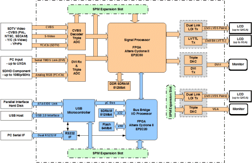
The CADIZ3500 mainboard is a dual-channel (dual-input, dual-output) graphics and video processor based on Altera Cyclone II EP2C50 and EP2C20 devices. It accepts a wide range of analog inputs including composite (CVBS), S-Video, HD/SD component and PC Graphics (RGB). A DVI receiver supports digital input signals. CVBS, S-Video and analog component inputs are decoded into digital YCbCr with the ADV7189B video decoder/digitizer. HD (1080p/60Hz) and
PC(UXGA) signals are digitized using AD9887A.
Any two input signals can be selected for further processing. The selected signals are available to the main-board “signal processing FPGA” and to the optional add-on card through the SPM expansion slot. Therefore the two selected signals can be processed independently by the optional add-on card, or the signal processing FPGA or simultaneously by both. The expansion slot allows the partitioning of large and complex designs or the addition of additional I/O and features. The two selected input signals can now be processed and be outputted simultaneously or be merged into a single multi-picture output (PIP, PAP, POP). Each of the output signals can be overlaid with an OSD. The output signals are available as High-Definition RGB/YPbPr (analog), SD video RGB/YPbPr (analog), analog PC graphics and DVI signal formats. The CADIZ3500 platform also supports direct connection to flat-panel displays via dual link LVDS, or 24-bit LVTTL interfaces. For superior performance and highest flexibility DDR SDRAM memory connected to the FPGA can be used for multi-frame image storage, allowing the implementation of high-performance 3D temporal image processing tasks.

Click to enlarge
1.2 Microprocessor section (Bus Bridge FPGA)
The Cadiz platform provides a full featured microprocessor subsystem. The subsystem consists of an on-board dedicated 8051 compatible CPU and the “Bus Bridge FPGA”. The 8051 compatible onboard CPU provides high-speed USB2.0, RS232 and EIDE (hard disk drive, HDD) interfaces. The dedicated 8051 CPU is sufficient for all housekeeping tasks and most of the applications. However sophisticated graphical user interfaces will most likely require more processing power. For these type of applications the Bus Bridge FPGA can be used to implement a 16-bit or a 32-bit microprocessor subsystem (i.e. Nios II platform). In this example a Nios II processor has been implemented. Nios II is a configurable 32-bit soft core from Altera. The Nios platform can be customized to the specific application. Altera offers a library of peripherals for the Nios II processor system. These peripherals can be connected easily. The microprocessor subsystem also includes
SDRAM, and parallel Flash. An expansion slot is also available to the microprocessor subsystem. The expansion slot could be used to implement additional peripherals such as 10/100/1000Mbit Ethernet, or to add keyboard functionality, remote control, or an LCD display.
2. HIERRO Add-on Cards:
The Cadiz platform is supported by additional add-on cards. These add-on cards can be easily plugged into the CADIZ mainboard. The HIERRO DSP cards are either based on Altera Stratix III, or Xilinx Virtex II PRO high-performance FPGA devices. The HIERRO DSP cards enable the platform to process memory-intensive applications such as video clip storage, and very complex 3D video algorithms. Additional add-on cards support audio signal processing, image sensor interfacing and provide extended I/O capabilities.
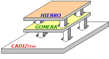
Designs can be partitioned across the mainboard signal processing FPGA and the add-on card FPGA’s. Specific add-on cards can also be stacked on top of each other. For example the audio card could be stacked on top of the video processing add-on card or an additional I/F card can be added to a video add-on card.

CADIZ Mainboard stacked with HIERRO and GOMERA add-on card's
3. IP Packages:
Various IP libraries are available for the CADIZ3500 platform. The CADIZ3500 IP library consist of Video IP Library (VLib), Memory Controller Library (MLib) and the Audio IP Library (ALib). VLib for example includes noise reducers, video scalers and de-interlacers, and graphic engines. The memory controller library (MLib) contains various SDRAM, DDR and DDR2 physical and application specific layers. The audio library (Alib) contains professional audio encoders, decoders, mixers and delay lines. Most IP blocks are configurable to meet specific performance requirements.
3.1 Video IP Library (VLib):
- HDSCALE1: HDTV/PC Scaler(720p/1080i/SXGA)
- HDSCALE2: HDTV/PC Scaler, (720p/1080i/1080p/UXGA); DDR SDRAM based
- HDSCALE3: HDTV Scaler (720p/1080i/1080p/UXGA); SRAM based
- DEINT1 : HDTV/SDTV De-interlacer
- DEINT2 : 2D HDTV/SDTV De-interlacer
- MOTIONANA: 2D Motion Analyzer / Detector
- NOISERED1 : 1D temporal Noise Reducer
- NOISERED2 : 2D Spatial Noise Reducer
- NOISERED3 : 3D Noise Reducer
- IMAGE_YENH : Y Image Enhancement Unit
- IMAGE_CENH : C Image Enhancement Unit
- HDMATRIX : HDTV/SDTV Color Space Converter
- HDMIX: HDTV/SDTV/PC Mixer
- HDOSD: High Resolution OSD Unit
- MULTIWIN: Multi-Window Display Controller
- HDSDVGC: HDTV/SDTV Video to Graphics Converter
- DCEPR1: High-Quality HD/SD Video/Graphics Data Compression Encoder
- DCDPR1: High-Quality HD/SD Video/Graphics Data Compression Decoder
- MCSRAM: SRAM Memory Controller, supports up to 72 Mbit synchronous SRAM devices (single data rate); configurable data bus width (up to 200MHz clock)
- MCSDR: SDRAM Memory Controller, 128/256/512 Mbit SDRAMs; up to PC133 spec
- MCDDR: SDRAM Memory Controller, 128/256/512 Mbit and 1 Gbit DDR SDRAMs; up to PC400 spec (200 MHz clock)
- MCDDR2: DDR2 SDRAM Memory Controller, 128/256/512 DDR2 SDRAMs (4 bank devices), up to PC667 (333MHz) spec
- DBFSC: Double Buffered Frame Store Controller
- TBFSC: Triple Buffered Frame Store Controller
- FPMC: Flex Port Memory Controller
- VIDFMT: HD/SD Video I/O Formatter
- AUDFMT: Audio I/O Formatter
- AESENC: AES audio encoder; supports also S/PDIF
- AESDEC: AES audio decoder; supports also S/PDIF
- AUDDLY: Audio delay line (up to 16 channels); up to 24-bits per sample; SDRAM based
- AUDMIX: 16 channel audio mixer; up to 24-bits per sample
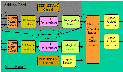
The following block diagram demonstrates how specific IP blocks can be picked from the library and put together to create a specific application. In this example two high-quality HD channels have been created. Each channel can process an incoming high-definition video stream independently. In each channel a scalable noise reducer measures the amount of noise in the selected input video signal and controls the settings of the digital noise reduction filters. After noise reduction, interlaced video signals are de-interlaced and scaled to meet the requirements of the respective progressive display (i.e. LCD, PDP).

Design Partitioning : Dual-Channel High-Definition Video Processor
If desired each stream can be overlaid with Graphics. The two video streams can be merged into a single video stream and be outputted on a single display (PIP, PAP, POP), or each of the streams can be outputted simultaneously on two separate displays. In order to implement this application, the HIERRO add-on card and an additional I/O card (GOMERA) providing a second HD input (DVI) has been used. One of the channels has been implemented by utilizing the mainboards signal processing FPGA, whereas the second channel has been implemented by utilizing the FPGA on the add-on card. Due to the expansion slots, the mainboards DVI and HD component input signals are available to the HIERRO FPGA. The HIERRO FPGA has also access to the GOMERA DVI input. The mainboards signal processing FPGA can select an HD signal from the mainboards DVI or HD component input, as well as the DVI input from the add-on card.
5. Design Methodology:
Altera Quartus II software has been used to compile and map the design to the respective FPGA’s (mainboard and add-on cards). All IP blocks have been written in Verilog code and have been simulated with the ModelSim simulator. SOPC Builder has been used to create the Nios II microprocessor subsystem.
6. Conclusion:
Due to the nature of video signals and the vast amount of data that needs to be processed and transferred, most applications can not be implemented by using standard DSP’s. These applications require one or more dedicated high-bandwidth and high-performance video signal processors. Most typical high-volume consumer applications are cost sensitive and are better addressed with the usage of a dedicated ASIC. However the ever increasing cost associated with developing an ASIC and the long development cycles do not work for many of the applications. These applications are better served by using FPGA based platforms. The ever increasing gate count and performance combined with the attractive pricing of today’s high-performance FPGA’s has enabled the rapid development of complex systems at an attractive price point. The above described scalable and configurable FPGA based platform is addressing these problems by allowing add-on cards to meet application-specific feature and performance requirements. In addition users can select and configure a variety of IP blocks from the Video-, Audio- and Memory- Libraries and build a customized solution. The software libraries provided with the platform support the configurability and a fast design cycle.
Related Semiconductor IP
- NPU IP Core for Mobile
- MSP7-32 MACsec IP core for FPGA or ASIC
- UHF RFID tag IP with 3.6kBit EEPROM and -18dBm sensitivity
- NPU IP Core for Edge
- Specialized Video Processing NPU IP
Related White Papers
- Programmable network processing blade needed in switching platform
- Configurable Processors for Video Processing SOCs
- Using vector processing for HD video scaling, de-interlacing, and image customization
- Video and image processing design using FPGAs
Latest White Papers
- Ramping Up Open-Source RISC-V Cores: Assessing the Energy Efficiency of Superscalar, Out-of-Order Execution
- Transition Fixes in 3nm Multi-Voltage SoC Design
- CXL Topology-Aware and Expander-Driven Prefetching: Unlocking SSD Performance
- Breaking the Memory Bandwidth Boundary. GDDR7 IP Design Challenges & Solutions
- Automating NoC Design to Tackle Rising SoC Complexity