FAUST: On-Chip Distributed SoC Architecture for a 4G Baseband Modem Chipset
Grenoble, France
Abstract:
The 10 X increase in complexity for the future 4G telecommunication terminals is a major challenge for system designers. SoC solutions seem the only answer to cope with the performance requirements, but the usual design practices lead to huge difficulties, especially for the implementation of the control schemes.
We describe our SoC implementation of a baseband subsystem for a high performance 4G terminal. Our architecture, called FAUST, is based on distributed synchronization and asynchronous communication. We highlight how we have actually implemented these two key principles in our design. We detail their impact in terms of complexity and the new constraints it introduces to the synchronization schemes. Finally, we illustrate the new control scheme with the timing diagram of an actual reception sequence.
I. INTRODUCTION
The increase in the complexity of future 4G mobile terminals is a major challenge for system designers. In particular, we expect a factor of 10 for the intrinsic complexity of new baseband modems. IP based design is still the solution, but the complexity of data synchronization and control imposes to re-consider usual design practices. We have implemented an architecture based on the aggregation of self-timed cooperating functional units. Data exchanges follow a distributed protocol and circulate on a high throughput meshed network. As a result, some of the intrinsic complexity is moved out from the individual functional units. On the other hand, the system behaves in a less deterministic way. We focus here on the distributed control aspect of our architecture. We briefly address the new problems encountered and some of the methods we have used for the design of a high performance baseband modem for 4G telecommunication.
II. FROM 3G TO 4G
4G systems, such as those currently prototyped in the framework of IST programs like MATRICE [8], 4MORE ([1],[10]), WINNER [9], are designed for data rates up to 100 Mbps. This is a major step compared to 3G systems, as defined by the 3GPP (and 3GPP2) projects, which allow aggregated data rates up to 2 Mbps. This performance increase has a dramatic impact on the complexity of new terminals, especially on the baseband processing part. The new challenge met by designers is twofold: some new IPs may be intrinsically very complex. But in addition, the functional chain is getting richer and less regular, and the option of a centralized control is not viable any more.
A. New mobile terminals must be flexible
For many reasons, such as time to market, standards evolution, interoperability, etc. flexibility is not an option for 4G terminals. Future mobile terminals should adapt with evolving standard. Ideally, these terminal architectures should allow for the combination of PHY layer data processing units in any arbitrary sequence. Designing a monolithic control to handle multiple combinations is not feasible.
B. Motivation for an ASIC-based Baseband Modem
Current baseband implementations for GSM, GPRS are digital signal processor (DSP)-centric, i.e. the DSP core performs the source codec function and most of the physical layer waveform processing.
In the case of 4G high data rate communication, only a small part of the baseband processing can be handled by such a DSP or a processor core. This invalidates the previous hardware/software split which was used for UMTS (3G) as well as for GSM (2G).
Thus, in such architectures, most of the baseband operations are still to be executed in hardware dedicated functional units. In the case of a discrete component implementation, this leads to a bus traffic bottleneck on the board and also contributes significantly to the power consumption. The only viable alternative is to integrate all components, i.e. CPU, DSP, dedicated hardware units and even memory on System-on-Chip (SoC) [2].
Furthermore, on the other key aspects such as power dissipation and price, there is no doubt that a dedicated hardware outperforms an architecture based on DSP component ([3], [4]).
III. THE FAUST APPROACH
FAUST, which stands for Flexible Architecture of Unified Systems for Telecom, is an architectural concept initiated in 2003 for supporting multiple OFDM air interfaces in a single SoC. It was developed originally with IEEE 802.11a and MATRICE in mind, and it was naturally extended to the 4MORE mobile terminal baseband implementation.
A. Design principles
Our architecture obeys to two driving principles:
1) De-correlation of data processing and data moving
For data processing, we implement a chosen set of key basic building blocks in a flexible and efficient way as independent functional units. Thus, differing data processing can be implemented just by combining these blocks in (almost) any arbitrary order. Data processing, done in the blocks, is de-correlated from data transport and data manipulation. Transport is organized around a layered protocol on top of a 2D meshed network.
2) Asynchronous communication
At functional level, the control scheme systematically uses a mailbox scheme to avoid any synchronous communication. At lower level, bit-level communications between units is based on dedicated un-clocked mechanisms, to preserve immunity to timing and frequency.
B. Coarse grain partitioning for flexibility
The flexibility challenge of our architecture is to obtain the right balance between implementation efficiency and versatility. This is true at the global system level: the system has to be partitioned in a way that most functional units may be reused for different applications. This is also true at the level of each functional unit, which is configurable enough to support multiple applications at a minimum complexity cost. Any specific baseband processing flow is implemented on the architecture in two steps: first, the algorithms are mapped onto combinations of “generic” functional units and data manipulation operations. This is not straightforward and may involve rethinking the operation to save memory or latency. The second step is to organize the data control flow (e.g. joins and forks). The way to implement the control flow in a distributed fashion is detailed in following paragraph.
Practically, our set of blocks span from generic vector arithmetic like vector multiplication to more OFDM specific functions such as FFT, etc. Pure data manipulation is specifically handled by a dedicated micro-programmed engine, called the DMA engine, which allows any arbitrary re-arrangement.
The terminal switches between two baseband protocols by switching its control software (CPU and/or lower level software), by changing its routing paths and re-initializing the configurations of its functional units.
C. The on-chip communication protocol
The communication between blocks is in fact the key of the whole architecture of the SoC. Data communication adhere to a protocol called the NoC protocol. The protocol may be summarized as follows:
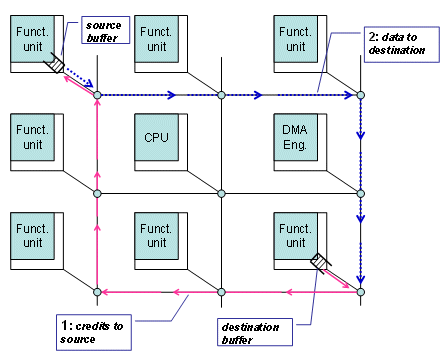
Regarding physical and data-link layer related aspects, the NoC protocol is based on a 2D meshed topology, through which the data flow is routed between the functional units in a programmable way [5]. All functional units are equipped with input and output buffers, visible on Figure III 1 below.
For on-chip communication, data retransmission overhead is not affordable. Thus, there can not be any data loss in the transport. Thus, data transfers may only happen when there is enough space in the recipient’s input buffer. To guarantee this, i.e. the safeness of data transfer on the network, we have added a communication mechanism that regulates data traffic and avoids the need of data retransmission. This mechanism is based on the exchange of “credits”, i.e. signaling messages from destination to source allowing the source to send packets.

Figure III 1 : data and credit flow
The mechanism is intrinsically simple: Before forwarding packets, the sender needs to receive credits from the receiver. At various times, the receiver sends credits to the sender, indicating available receive buffer size. As represented above, credits may follow another route than the data. The price to pay for this mechanism is an additional complexity in managing the credits, and a risk of functional interlocking.
D. Distributed synchronization
1) Principle
The combinatorial of the baseband progressing is such that the classical ASIC design approach, which consists to implement the function as a hierarchy of FSM coupled with data paths, is not feasible. It would be very difficult to develop and impossible to maintain, since any small change would require a change of the complete system. This is our main motivation to adopt a distributed and data synchronized approach. The baseband processing is implemented as a self-synchronized data pipe-line. Data moving is implemented in hardware, used as a low-level synchronization means.
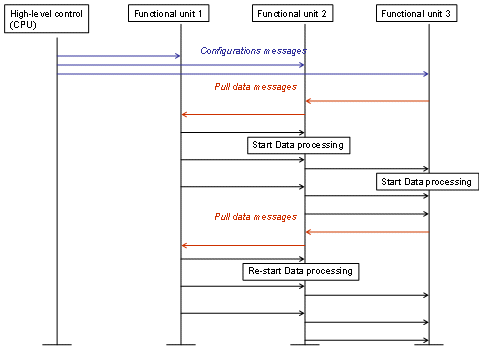
In other words, the SoC data path is globally organized as a pipe-line: data packets are pulled regularly from sources by the destinations. Every functional unit includes FIFO buffers to handle incoming and outgoing data.
2) Data sequentialization
Each functional unit has enough autonomy to perform its processing. The functional unit synchronizes locally with its data sources and sinks: the processing is triggered by the arrival of data, and stops whenever there is no more data to process, or when the destination can not accept any more data.

Figure III 2 : FAUST generic synchronization mechanism
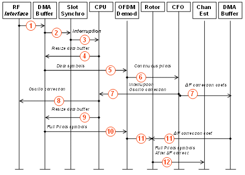
In contrast to this “local” synchronization, “global” synchronization is kept to a strict minimum, and assumed via software by the embedded CPU, using interruptions. A typical example is shown on figure IV-2, where the CFO unit triggers a complex correction sequence by interrupting the CPU. This solution ensures maximum flexibility and acceptable performance, since such interruption happen seldom (once a frame), and do not interfere with the data processing critical path.
However, a typical 4G baseband processing can not be simply reduced to a regular pipe-line: in most of the functional steps, data has to be sequentially sorted and submitted to distinct sinks. On the other side, some processing unit require data from different sources in a fixed order. When necessary, this sorting and dispatching of data is handled by the DMA engine, using a specific data buffer and its associated microprogram. This mechanism is described in section E.
3) Immunity to delays
The Functional unit cores are wrapped by standardized network interfaces (appearing in white on Figure III 1) which buffer incoming and outgoing data. Therefore, the cores can fully ignore the exact arrival date of data. This makes the system “loosely coupled” and thus easier to modify without changing the global result of the processing. The price to pay is the addition of data FIFOs as input and output of each functional unit, plus, marginally, extra latency in the communication.
E. Firmware for data manipulation
Most of data handling follows the very same patterns: blocking or non blocking FIFO, regular data re-arrangement. Mutualization is therefore obviously a gain in complexity since it avoids duplication. Thus, we use the DMA engine, a dedicated micro-programmed controller, to handle these aspects. This “soft” data management has huge advantages: It is capable or arbitrary re-arrangement of data, and thus it realizes at minimum cost basic baseband functions such as framing, deframing, separation of pilot data, interleaving, or even some spatial multiplexing schemes. It implements natively blocking FIFOs which avoid the need of complex synchronizations, and do not require any mutual exclusion mechanism. Least but not least, data manipulation is programmed in a C-like syntax, which insures readability, and manageability. On the other hand, it requires the design of a complex data processor, and the development of a dedicated compiler.
F. Impact on the system design
1) Impact on complexity
Clearly, our architecture shifts the complexity out of the functional unit but increases the global transition graph of the system.
It decouples the different data processing functions, at the cost of extra hardware for the network and the “wrapper” interfaces.
2) New constraints
The NoC implementation imposes other constraints on the communication schemes:
- Because of its switched structure, it is not well suited for read operations: thus, all SoC operations are based on combinations of write and write-back operations.
- There is no global ordering guaranty for data transfers. Packets emitted by different sources may overpass each other in the network. However, transfers from a same source to a same sink stay ordered.
- There is no acknowledgement for a write operation. Thus, sequentialization of data between different sources has to be done at the destination, by using the credit mechanism to trigger the data flows in the right order.
- Packets always arrive to their destination, but there is no guarantee of delay.
3) New problems: functional deadlocks, throughput, power consumption policy
The FAUST architecture makes the design globally more manageable, but introduces new requirements to the system designer, who must pay attention to new problems:
- Functional deadlocks: whereas the routing scheme guarantees the liveness of data routing, it is possible to introduce starvation in the system with incorrect data regulation policies. We used the SPIN [7] system for formal verification in our case.
- Throughput: data latency on the NoC may vary according to the network topology and to the functional scenario: we used a modified version of NS2 in our case for evaluating the latencies and link saturations of our applications [6].
- Power consumption: instrumentation for power adds a new dimension to the design. It becomes possible to reduce the frequency or the voltage of any functional unit without changing the global functionality of the application.
IV. FROM CONCEPTS TO DEMONSTRATOR
A. Hardware demonstrator structure
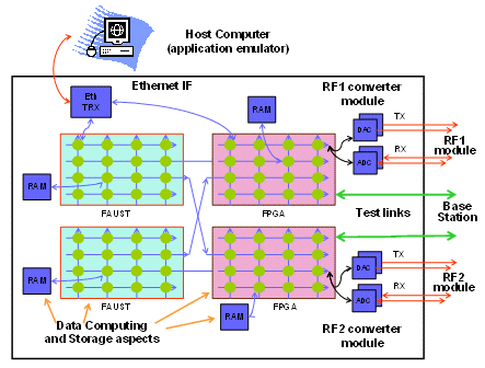
To validate the concepts presented in this paper, we have developed a first IC (the “FAUST chip”) and a complete open NoC-based platform based on both FAUST and FPGA components has been designed (see Figure IV 1). This platform is primarily targeted for the 4MORE mobile terminal demonstrator. We have extended the SoC network to a FPGA, as shown in Figure IV 1 below, because we wanted to cover a large class of telecom baseband solutions. The FPGA holds very specific, non timing critical functional units such as frequency tracking, specific I/F to RF, etc. However, the network implemented on FPGA is physically different (e.g. synchronous) but fully compatible with the on-chip structure. Thus, a final end-user market SoC implementation may be obtained by simply shifting the FPGA blocks inside the chip.
The prototyping platform features two ASIC and FPGA couples. It includes provisions for instrumentation: computing resources, memories, Ethernet interfaces, clock generators, I/Q analog and digital interfaces, debug and monitoring features.

Figure IV 1: Mixed on-chip and off-chip Platform
Functionally, the platform implements the usual features of a wireless communication modem. More specifically, it is tuned for MIMO MC-CDMA modulation for data rates up to 100 Mbps. It features:
- Carrier and packet detection, by means of correlation and equalization.
- Modulation and demodulation: it implements OFDM schemes associated with spectrum spreading.
- Mapping and de-mapping, using different constellations.
- Channel coding and decoding, using various codes, puncturing and programmable interleaving.
- Configurable hardware implementation for most functions: FFT, Viterbi coding, interleaving, mapping, scrambling, puncturing, etc.
- On-chip processor to add arbitrary functions to the data processing flow.
- Programmable MAC control.
B. A sequence example
The diagram on Figure IV 2 illustrates typical features of our architecture: the punctual role of the CPU to manage a buffer and the beginning of reception, the usage of micro-programs to sort data in sequence and the usage of data credits to synchronize the sequence of operations.

Figure IV 2: Rx sequence schedule
The 12 steps illustrated here are:
- RF/BB interface is active, data is continuously sent to a DMA buffer
- In this step, data is forwarded to the unit in charge of identifying the slot synchronization symbol.
- When found, an interruption is issued.
- The CPU calculates the actual beginning of frame and re-aligns the buffer pointer.
- Then, it sends selectively data symbols (including continuous pilots) to the OFDM demodulator (FFT)
- Only continuous pilots are transmitted to the carrier frequency offset tracking unit.
- Once frequency offset is obtained, correction is computed and an interruption is generated. Correction values after FFT are stored in another DMA buffer (30 values, 1 per symbol).
- The CPU updates the frequency of the RF/BB interface, which will be transferred to the VCTCXO at the end of the current slot.
- The CPU eventually corrects the pointer buffer.
- Then, it sends selectively full pilots symbols to the OFDM demodulator (FFT).
- Full pilots symbols are transmitted from FFT to rotor unit for frequency offset correction. Correction values are read from a DMA buffer.
- Corrected full pilots are sent to channel estimator.
V. CONCLUSION
The FAUST architecture is in fact a design framework for complex SoC systems. This approach simplifies the design at RT level, at the price of some constraints at higher levels. Our experience of a complex 4G baseband system shows the validity of our approach for telecommunication systems. Specifically, it is a promising approach for the effective implementation of Software-Defined Radios (SDR).
More broadly, we think it is well adapted to data-intensive, irregular computation. However, like any truly distributed system, it requires extra care in the implementation. It introduces new dimensions to the design space, e.g. topology optimization, network performance, power control, and new constraints in the global synchronization schemes, which will force SoC designers to adopt the structured approaches used in complex software systems.
ACKNOWLEDGMENTS
The work presented here was carried out in the project 4More (4G MC-CDMA multiple antenna system On chip for Radio Enhancements) that is supported from the European Commission in the framework of FP6 with the contract number IST-2002-507039. The authors would like to acknowledge for this support and the possibility to carry out the research work.
REFERENCES
[1] Stefan Kaiser et al. “4G MC-CDMA Multi Antenna System on Chip for Radio Enhancements (4MORE)” IST summit, Lyon, June 2004
[2] Friedbert Berens, Yves Durand, Fabienne Nouvel, Stefan Kaiser “Designing a multiple antenna MC-CDMA SoC for beyond 3G”, in Embedded Systems Conference, San Francisco, March 2005
[3] Josef Hausner, "Integrated Circuits for Next Generation Wireless System" in Proc. of the European Solid-State Circuits Conference (ESSIRC), 2001
[4] D. Greifendorf, J. Stammen, and P. Jung, “The evolution of hardware platforms for mobile software defined radio terminals,” in Proceedings of the IEEE Personal, Indoor, and Mobile Radio Conference (PIMRC), Lisbon, Portugal, Sept. 2002
[5] F. Clermidy, D. Varreau, D. Lattard “A Noc-based communication framework for seamless IP integration in complex systems” IPSOC 2005
[6] R. Lemaire, F.Clermidy, Y. Durand, D. Lattard and A. Jerraya “Performance Evaluation of a NoC-Based Design for MC-CDMA Telecommunications using NS-2”, in RSP’05 Intl Conference, 2005
[7] The SPIN model checker, available at http://spinroot.com/spin/
[8] MATRICE project web page, available at http://www.ist-matrice.org/
[9] WINNER project web page, available at https://www.ist-winner.org/
[10] 4MORE project web page, available at http://ist-4more.org/
Related Semiconductor IP
- NPU IP Core for Mobile
- NPU IP Core for Edge
- Specialized Video Processing NPU IP
- HYPERBUS™ Memory Controller
- AV1 Video Encoder IP
Related White Papers
- Power Management for Internet of Things (IoT) System on a Chip (SoC) Development
- A short primer on instruction set architecture
- UPF Constraint coding for SoC - A Case Study
- Integrating VESA DSC and MIPI DSI in a System-on-Chip (SoC): Addressing Design Challenges and Leveraging Arasan IP Portfolio
Latest White Papers
- Ramping Up Open-Source RISC-V Cores: Assessing the Energy Efficiency of Superscalar, Out-of-Order Execution
- Transition Fixes in 3nm Multi-Voltage SoC Design
- CXL Topology-Aware and Expander-Driven Prefetching: Unlocking SSD Performance
- Breaking the Memory Bandwidth Boundary. GDDR7 IP Design Challenges & Solutions
- Automating NoC Design to Tackle Rising SoC Complexity