Debug and testability features for multi-protocol 10G Serdes
Prism Circuits Inc., Santa Clara CA, U.S.A.
Abstract :
The paper describes the design-for-test (DFT) features of a 10.3125Gb/s Serdes and other such high datarate IP as XAUI, PCIe, and others. It is shown that extensive testability can be implemented in a high data-rate Serdes. The paper describes the bench-test and characterization features, as well as wafer and production test considerations. The Serdes is compliant to IEEE 802.3ap. The DFT features include IEEE 1149.6 AC boundary scan, PRBS generators and checkers. Methods for observing both internal analog and digital nodes inside the Serdes are discussed. Loopback circuitry includes an on-die “stressed-eye” feature that can adjust both the amplitude and timing of the loopback waveform through a programmable code. An internal eye monitor features allows the system designer to view the eye as it is seen by the receiver.
Keywords: 10.3125 Gb/s Serdes IP, design-for-test, IEEE 1149.6 compliance, stressed-eye loopback, internal-eye-monitor.
1. Introduction
Rapid qualification and testing of high data rate Serdes IP, while very challenging, is crucial in managing product cycle times. Our paper describes the testability and debug features included of a 10.3125Gbps Serdes, including all levels of analog and digital tests which are used during several stages of product manufacturing. We will describe the techniques which allow us to incorporate these features without compromising normal operation.
We begin by providing an overview of the Serdes in Section 2. In following sections we describe the features that enable bench-, wafer-, and production-test. These features will be shown to be important aspects of screening a high-speed Serdes IP.
2. SERDES Implementation Background
Our DFT is built into a Serdes design implemented using Fujitsu’s 65nm technology and operates with a bit-error-rate of 10^-12. A high level block diagram of the is shown below:
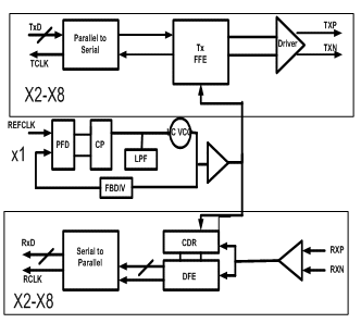
Figure 1 SerDes Overview
The design consists of a global clock-generation unit, with distributed transmitter (Tx) and receiver (Rx) portions. A macro can support two to eight transmitter/receiver pairs. The digital logic layer is provided separately as a soft macro. To achieve the 10.3125 Gbps specifications we rely on:
- Current mode output drivers, with 3-tap TX feed-forward-equalization (FFE),
- Extensive calibration (i.e. Adaptation, termination calibration, offset tuning),
- Linear equalization and decision feedback equalization ,
- LC tank VCO PLL (low power and jitter),
- Low latency design,
- A floorplan designed to benefit the clock distribution.
We have provision for directly controlling the phase of the recovered clock and also the offset of the input samplers.
The Serdes meets the ‘IEEE 802.3ap Ethernet Over Backplane’ and supports:
- 4 x 10GBASE-KR PMD
- 10GBASE-KX4
- 4 x 1000BASE-KX PMD
- PCI-e Gen2
- 3.125 Gbps XAUI
Other data rates are possible, including (but not limited to) ½ Data Rate (5 Gbps), ¼ Data Rate (2.5Gbps), ⅛ Data Rate 1.25Gbps and 0.78125 Gbps.
3. Debug and Testability Features
The following section describes the testability features employed by the Serdes. The features are used to support :
- Bench-test and system bring-up,
- Wafer-screening of unpackaged parts,
- Full production test
3.1 Bench-testing and System Bring-Up
Observability and programmability are critical to both rapid system bring-up, and to verifying that circuit performance meets expectations. In order to achieve 10.3125 Gb/s data rate, the Serdes sub-blocks are given tight specifications for timing and jitter, supply noise rejection, offset, linearity, and duty-cycle.
PLL locking and phase-jitter performance are among the first things that need to be observed. We drive the PLL clock to a high-speed transmitter output (see Figure 2), using a precision time base as the oscilloscope trigger.
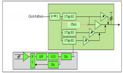
Figure 2 PLL drives a transmitter. The RMS jitter < 600fs at 5-GHz
This enables quick confirmation of frequency locking, phase jitter, and loop bandwidth. For the LC PLL we observed < 600fs of RMS jitter at 5-GHz, indicating that the design was well suited to our application. The test does not compromise the normal operation. To ensure the design meets specification in a system environment it is best to perform these tests with in a noisy environment with several active channels and PLL’s.
Other critical high-speed nodes are visible through a digital monitor unit (DMON). Critical signals are buffered, multiplexed, and brought off-chip through a high-speed transmitter to a dedicated bump. This technique is used to make high-bandwidth measurements of several critical high-speed nodes including:
- Phase interpolator outputs (for to determine linearity and phase spacing),
- Several points on the clock tree (to establish the jitter profile),
- Analog-front-end and continuous-time-linear-equalizer (CTLE) outputs.
A similar method is employed to verify analog voltages. Analog multiplexors choose a voltage and drive a unity-gain amplifier to a dedicated bump. This allows the system designer to confirm that the analog biasing meets expectations across skew corners. The following can be observed:
- Power supply levels (after dividing by two using a resistive divider),
- Critical bias points,
- Bandgap reference voltage,
- Loop filter voltages for the timing control circuits.
These circuits and observation points are very useful for ensuring that the circuits work as expected across a large sample of parts.
The test-board includes several channels of varying materials and lengths. Using an octal configuration we drive a pattern through transmitter channels either to an oscilloscope or back to the respective receiver channels. The digital portion of the Serdes implements a PRBS pattern generator and checker per-lane. The PRBS generator is capable of generating five pseudo-random test patterns including :
- PRBS31 (similar to 64/66b),
- PRBS23 (to support old test equipment),
- PRBS11 (used by 10GBASE-KR link training),
- PRBS9 (used by 10GBASE-LRM),
- PRBS7(similar to 8b10b data)
In addition the Serdes can generate programmable pulse-width patterns (between 1 and 32UI) square waves. These can be used to drive variable width pulses (i.e. clock patterns) and DC data.
On the receiver side, the received PRBS pattern can be checked using the PRBS checker in the digital portion of the Serdes. The PRBS checker is connected to a 32-bit-error counter and a 48-bit timer. During loopback test, bit-errors can be injected into any transmit data stream on an independent per-lane basis. Each lane has a programmable bit-error interval counter and bit pattern.
The pattern generation mechanism is used in conjunction with the internal-eye-monitor (IEM) to derive the timing and amplitude margins. The IEM is software that sweeps :
- the phase of the recovered clock,
- the offset of the sampling flop,
and measures the bit-errors that have occurred over each time period.
These capabilities combined enable us to stress the Serdes, ensure that the design has good margin,
3.2 Wafer-screening and Production Test
Screening parts before they are packaged is a very important part of an overall test program. Good parts are then packaged and then tested in a production environment.
The portions of the Serdes covered by scan are shown in Figure 3. The digital portions, as well as the serializer/de-serializer, CDR and adaptation logic have full scan.
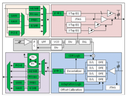
Figure 3 Digital sections are fully scannable, including the CDR
The Serdes has a provision to expose more of the analog functions at wafer-screen as well. This is achieved through on-die loopback. The loopback methodology is compatible with wafer level probing in the earlier stages, as well as full data rate test later on in the cycle. Support is provided for the following modes (see Figure 4):
- Near-end – loopback of the digital layer back to itself,
- Far-end #1 - loopback of the transmitter predriver output back into receiver front end,
- Far-end #2 – loopback of the transmitter driver output back into the receiver front end.
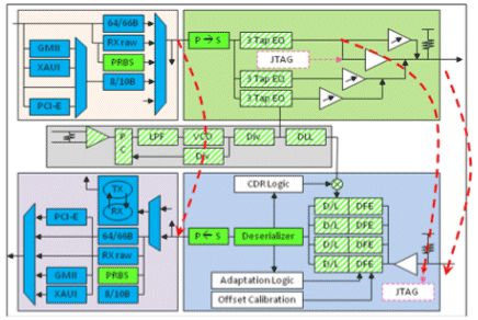
Figure 4 Three loopback paths on the Serdes, two of which feature stressed-eye filters.
The implementation of the loopback is critical to both it’s effectiveness, and it’s impact on normal operating modes. Excessive pad capacitance degrades timing margins.
Pass-transistor multiplexors isolate the Tx and Rx so that the additional capacitance is very small. For the far-end modes we have an option to stress the eye. The amplitude is varied through the native programmability of the transmitter amplitude. Modulating amplitude isn’t enough to reproduce the effects of typical channel because the eye height reduces, however the width isn’t as affected. Thus, a programmable filter is incorporated inside the loopback path and allows us stress the eye in both the width and height. It is possible to perform very thorough testing on a tester without a system board.
The Serdes is compliant to IEEE 1149.6 standard and contains full boundary scan. The boundary scan chain can be connected to the chip level boundary scan chain for ‘ IEEE 1149.6 Boundary Scan Test,’ (refer to Figure 5) below.
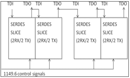
Figure 5 Connect slices together to form a single chain
Inside each slice there are a pair of observation-only boundary scan cells (BC_4) for each differential receiver and one output-only boundary scan cell (AC_1) for differential transmitter (see Figure 6).
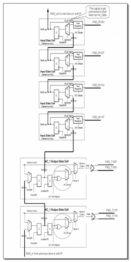
Figure 6 IEEE 1149.6 implemented in the Serdes Slice (1 slice is comprised of 2 data lanes).
4. Conclusions
The paper described the DFT features of a 10.3125Gb/s Serdes, including the bench-test and characterization features, as well as wafer and production test considerations. The Serdes is compliant to IEEE 802.3ap, uses scan extensively, and incorporates several loopback modes. We showed that extensive testability can be realized without compromising high-speed operation.
Acknowledgements
The authors wish to acknowledge the strong support of our foundry partners at Fujitsu Microelectronics, in particular Sakai Toshiaki, Toru Takaishi, and Yong Miao.
Related Semiconductor IP
- SerDes
- Automotive Grade PLLs, Oscillators, SerDes PMAs, LVDS/CML IP
- 112G Multi-Rate SerDes
- 100G SerDes PAM4 PHY
- 32Gbps SerDes PHY in GF 22nm
Related Articles
- How a 16Gbps Multi-link, Multi-protocol SerDes PHY Can Transform Datacenter Connectivity
- Co-Design for SOCs -> On-chip support needed for SOC debug
- Co-Design for SOCs -> Software debug shifts to forefront of design cycle
- Improving the Testability of Complex SoC Designs
Latest Articles
- Assertain: Automated Security Assertion Generation Using Large Language Models
- VolTune: A Fine-Grained Runtime Voltage Control Architecture for FPGA Systems
- A Lightweight High-Throughput Collective-Capable NoC for Large-Scale ML Accelerators
- Quantifying Uncertainty in FMEDA Safety Metrics: An Error Propagation Approach for Enhanced ASIC Verification
- SoK: From Silicon to Netlist and Beyond Two Decades of Hardware Reverse Engineering Research