Dose Mapper - Advanced System for Correction of Critical Dimension (CD) Variations in Deep Sub Micron Technologies
Deepak Sharma, Sachin Kalra, Azeem Hasan, Rahul Saxena ( Freescale Semiconductors)
Introduction:
Semiconductor industry is moving towards the deep sub micron technology where the channel length of the device becomes as small as 65/40/32/28 nm and beyond. Fabrication of these smaller devices is a big challenge due to critical dimension uniformity (CDU) which impacts the device performance and its characteristics. CDU is a major contributor to yield drop out in deep sub micron technologies and a big concern to the lithography process. Both the Intra field and the inter field type of CD variations can be controlled by an advanced system named as Dose Mapper which provides wafer CD feedbacks to the scanner.
This paper provides an update on Critical Dimension (CD) Variations, Dose Mapper System to maintain critical dimension uniformity (CDU) and Standard Cell Architecture of Dose Map Key.
Critical Dimension (CD) Variations:
In deep sub micron technology nodes such as 65 nm and lower, the critical dimensions (CDs) of many critical manufacturing layers are governed by the wavelengths of the UV light used in photo lithography and film thickness has approached atomic layer dimensions resulting in greater variability. Various steps of IC fabrication like lithography, optical and etching proximity effect, mask error etc. leads to a variability of around 10% in gate length critical dimension at 40 nm technology. A larger polysilicon (gate) critical dimension (CD) variation affects the product performance, power and leakage.
Deep sub micron technology nodes have very small transistor dimensions so it is very difficult to avoid the dopant fluctuations. At 65 nm technology node, the number of dopants in a transistor is less than 100 atoms which can increase the threshold voltage of the device. Even the dopant location is also important at these smaller dimensions.
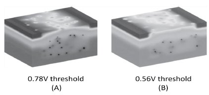
As shown in the Fig.1 threshold voltage of two transistors having the same number of dopants (170) can vary depending upon the location of the dopant atom.

Fig.1 Random Dopant Location results Threshold Voltage Variation
These different location patterns of the dopants depend upon the energy acquired by them at the time of ion implantation and it is very difficult to control this energy attained by the dopants. Process variability also impacts dopant uniformity across the device which reduces the parametric yield.
Technology nodes are shrinking but the wave length and numerical aperture (NA) of the UV light used in photo lithography process is still a major concern for the manufacturers. The result is that the process window is shrinking but the optical lithography process is not able to follow the Moore’s law. The illumination wave length has been stuck at 193 nm, because it is difficult to bring extreme ultraviolet scanners on line as listed in Table1.

Table1 Illumination Sources Available for Optical Lithography
Manufacturers and designers are continuously working to develop various processes and systems to overcome these CD variations in deep sub micron technologies. Resolution Enhancement Techniques (RET), Phase Shift Masking (PSM), illumination optimization are some of the processes taken in to consideration at the fabrication level to overcome CD variation. Dose Mapper system is also a smart and advanced system used by the designers and manufacturers to overcome the CD variations.
Dose Mapper System to Maintain Critical Dimension Uniformity (CDU):
Dose Mapper is an advanced dose control system with a real time graphical user interface, which allows the user to decide dose map configuration and exposure sensitivity to maintain the critical dimension uniformity (CDU) across the exposure field and wafer. Dose Mapper system is a major highlight of the Advanced Process Control implementation for real time control of production to improve yield.
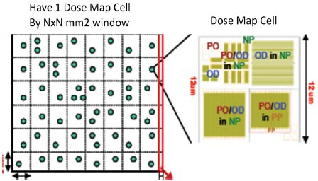
Dose Map cell is key to Dose Mapper System, which is verified by the manufacturer as per their experiments and analysis on a particular technology node. Dose Map cell has various poly and diffusion layer polygons and rectangles placed in a specified manner decided by the manufacturer. This Dose Map cell is placed uniformly in the SOC at Floor planning stage. If the chip is divided in windows of particular dimensions, then each such window must contain one Dose Map Cell as shown in Fig.2

Fig.2 Dose Map Cell distribution in the Entire Chip Area
Final GDSII contain the Dose Map Cells placed uniformly across the chip. A Unix based software checks the poly (gate) and diffusion (source and drain) of all the transistors placed in the chip taking the poly and diffusion inside the Dose Map Cell as reference and marks the places where the poly and diffusion of the transistor may create CD variations at fabrication stage. This is done so the designer can change the placement of the transistors at the design level itself and correct the potential yield loss. This Dose Mapper system is easy to use and is very cost effective.
Standard Cell Architecture of Dose Map Key:
Dose Map Key is the basic cell which consists of poly and diffusion polygons laid out in a specified manner which is approved by the manufacturer for that technology node. This cell is finalized by the fabrication lab as per the detailed analysis and experiments on CD variations carried out for the technology node. Fig. 3 shows an example of Dose Map Key cell of fixed height and length.

Fig.3 Dose Map Key of fixed height and length for a technology node.
SOC designers place this Dose Map Key cell uniformly throughout the chip during the floor planning stage in design implementation. The height of this cell is not the same as a standard cell so automatic placement and routing (APR) is not possible for this cell in standard cell rows. Therefore, this cell has to be placed and routed in a custom manner, which increases the complexity of implementation.
To overcome this limitation, the Dose Map Key cell can be laid out in the same fashion as a standard cell. This Dose Map Key cell is instantiated in a top cell which, again has similar foot print as a standard cell and follows all the boundary rules like the other standard cells in a cell library. This top cell is called as a Dose Mapper cell and this cell can be easily placed and routed by the PnR tools used in design implementation. Fig. 4 shows the Dose Mapper Cell which is standard cell format of the Dose Map Key cell.

Fig.4 Dose Mapper Cell which is Standard Cell Format of Dose Map Key.
Conclusion:
Dose Mapper system is an advanced and effective system to maintain the critical dimension uniformity (CDU) on the wafer. This system enables identification of intra field and inter field critical dimension (CD) variations at design level itself and facilitates correction in very easy manner at the design stage itself. Semiconductor designers and manufacturers are looking towards adapting the Dose Mapper system due to its high reliability and lower cost to achieve higher yields.
References:
1. A. Asenov, Random dopant induced threshold voltage lowering and fluctuations in sub-0.1 u, MOSFET’ s:a 3-D “atomistic” simulation study, IEEE Trans. Electron Devises, vol. 45, no. 12, pp. 2505 – 2513, Dec. 1998.
2. J. van Schoot, et.al. “CD uniformity improvement by active scanner correction” Proc. SPIE Vol. 4691, pp.304-314. 2002
3. C. Ausschnitt, “Rapid optimization of the lithographic process window”, SPIE Vol. 1088 (1989) pp. 115-123
Authors:
Deepak Sharma: Working at Freescale Semiconductors, India as Senior Design Engineer and 8 years of experience in Physical Design, Analog Layout Design and Standard Cell Library Design.
Sachin Kalra: Working at Freescale Semiconductors, India as Senior Design Engineer and 6 years of experience in Physical Design, Analog Layout Design and Standard Cell Library Design.
Azeem Hasan: Working at Freescale Semiconductors, India as Senior Design Engineer and 4 years of experience in Physical Design, Analog Layout Design and Standard Cell Library Design.
Rahul Saxena: Working at Freescale Semiconductors, India as Staff Design Engineer and 12 years of experience in Physical Design, Analog Layout Design and Standard Cell Library Design.
Related Semiconductor IP
- NPU IP Core for Mobile
- NPU IP Core for Edge
- Specialized Video Processing NPU IP
- HYPERBUS™ Memory Controller
- AV1 Video Encoder IP
Related White Papers
- Why the Memory Subsystem is Critical in Inferencing Chips
- The Future of Embedded FPGAs - eFPGA: The Proof is in the Tape Out
- A Standard cell architecture to deal with signal integrity issues in deep submicron technologies
- A Basic Analysis of Interwire Capacitance in Ultra Micron Technologies
Latest White Papers
- Ramping Up Open-Source RISC-V Cores: Assessing the Energy Efficiency of Superscalar, Out-of-Order Execution
- Transition Fixes in 3nm Multi-Voltage SoC Design
- CXL Topology-Aware and Expander-Driven Prefetching: Unlocking SSD Performance
- Breaking the Memory Bandwidth Boundary. GDDR7 IP Design Challenges & Solutions
- Automating NoC Design to Tackle Rising SoC Complexity