A Basic Analysis of Interwire Capacitance in Ultra Micron Technologies
Trisha Ghosh, Rishabh Agarwal, Vishant Gotra (Freescale)
ABSTRACT
As the technology node decreases, meeting inter-wire or coupling capacitance becomes extremely critical and challenging in SOC design. Shrinking technology node leads to increase in dielectric values, thus leading to higher capacitance and hence an increase in inaccuracies and power. In this paper, we propose effective ways to reduce interconnect capacitance in ultra micron technologies.
INTRODUCTION
As the technology node decreases, the challenges for the layout designer also increase. Shrinking technology node leads to an increase in dielectric values, which leads to an increase in capacitance. Transistors can be scaled down in size such that the device delay decreases in direct proportion to the device dimensions. But the case is not the same with interconnects. For submicron-geometry chips, it is the interconnect delays, rather than the device delays that determine chip performance. If the interconnects are scaled down, it results in RC delays that begin to dominate the chip performance.
In this article we discuss the different types of capacitances encountered in ultra micron technology between interconnects. We also describe in detail the shielding of analog routes with the effect of capacitance and a few ways to reduce the capacitance. We also provide an idea concerning metal layer usage topology in accordance based on need and the application.
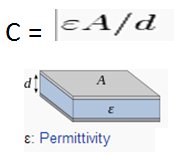
BASIC FORMULA TO CALCULATE PARALLEL PLATE CAPACITANCE

FIG1. Parallel Plate Capacitor
In sub-micron technologies (greater than 90nm), only area capacitance is taken into calculation and we ignore coupling and fringe capacitance, but in deep sub-micron technologies (less than 65nm) 2D-3D fringe, coupling and area capacitance is also included.
WHY CAPACITANCE INCREASES WITH DECREASING TECHNOLOGY NODE
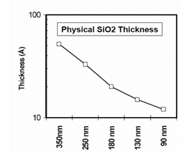
SiO2 has been the preferred gate insulator for silicon MOSFET since the 1960’s. Over the years, the oxide thickness has been reduced from 300nm for 10µm technology to 1.2nm for 65nm technology.
There are two reasons for the relentless drive to reduce the oxide thickness.
- A thinner oxide, i.e. a larger Cox raises I-on. A large I-on is desirable for maximizing the circuit speed.
- To control Vt roll-off (and therefore the sub-threshold leakage)

FIG2. Decreasing Trend in Oxide Thickness with Decreasing Technology
EFFECTS OF INCREASING CAPACITANCE
- INCREASE IN POWER – Increase in capacitance leads to increase in RC, and hence increase in chip power.
- INCREASED CROSSTALK BETWEEN ANALOG SIGNALS – As the capacitance of a given signal shoots its required specifications, its accuracy also increases.
- DIE AREA IMPACT – In order to meet capacitance specifications, the signals need to be spaced as far as possible. This requirement can lead to an increase in die area.
TYPES OF CAPACITANCE FORMED BETWEEN INTERCONNECTS
1. SELF CAPACITANCE (Metal to Substrate capacitance)
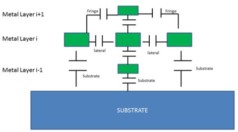
The simplest structure examined here is an isolated metal line over the silicon substrate. The capacitance formed between the substrate and any metal layer above is called self or area capacitance. Thus this capacitance is always formed. The value of this capacitance is dependent on two factors, length and metal layer used. Metal-oxide-silicon capacitance has slightly different characteristics than metal-oxide-metal. Small changes in capacitance can result due to inversion in the field regions or other substrate effects. This is an inherent advantage of measurement in the case of metal-to-substrate capacitances.
2. Mutual Coupling Capacitance (INTERWIRE CAPACITANCES)
Capacitance between metal lines of the same layer is referred to as inter-wire or coupling capacitance. This is a major problem in deep submicron technologies due to tighter pitch and higher metal aspect ratios. An undesired voltage spike resulting from this capacitive coupling is commonly referred to as crosstalk. The presence of another nearby line will increase the total capacitance of the isolated line. This added capacitance must be taken into account when routing global signals such as clocks, determining driver sizes and line widths/spacing etc.
3. Fringe Capacitance
Fringe capacitance is formed between non-overlapping sidewall of one conductor and surface/sidewall of a second conductor on the same or different layer from the first one. This type of capacitance becomes significant as we route in higher layers because higher layers are thicker.
For higher metal layers, inter-wire effects are more pronounced due to increased metal heights and lessened substrate effects. Since most signals are routed on lower levels, crosstalk is less critical in higher layers normally carrying power and ground. But sometimes while routing analog nets, signals having special requirements (like less resistance, crosstalk) need to be routed in higher metal layers. The method used to shield the special signal routes is to cover the upper and lower area of the signal route by other grounded metal planes. Although, this affects coupling capacitance, it helps in reducing any crosstalk with any other signal route. The grounded metal plane attracts all the disturbances in the form of electric fields which could have hampered the original signal originally. This is a trade-off between total capacitance and noise imputation.

FIG3.Types Of Interconnect Capacitances
WAYS OF SHIELDING INTERCONNECTS
The methodology used presently for shielding is that shield wires are tied statically to Vdd or ground. In this article, we explain the concept of coupling capacitance in terms of aggressor and victim. Many cases are explained here which will help in deeply analyzing the change in capacitance as the setup is changed. Each type of setup described below has its own benefits in term of reduction of crosstalk and coupling capacitance, but at the same time it can seriously affect metal availability for routing.
SETUP 1: When there is only one net drawn in layer n
As can be seen from the figure, the signal route is in the design in layer n. The capacitance value obtained for this route is because of the self area capacitance (metal-to-substrate capacitance). There is no other route in any other metal layer so there is no coupling and no fringe capacitance present. As stated earlier, eliminating this type of capacitance is difficult. This setup is most prone to noise and crosstalk, so sensitive signals are always shielded.
Ctotal = Cself
SETUP 2: When lateral shielding is performed in the design
As seen from the figure, there is a sensitive route in layer n which is shielded from both sides in the same metal layer n. In this type of setup, self area capacitance, fringe and coupling capacitance come into action. The self area capacitance is due to the formation of capacitance between the route and substrate. The coupling capacitance is due to the shields placed in the same metal layer n. Distance is indirectly proportional to the capacitance, so as the distance between signal and shield wires increases, coupling capacitance decreases. However, this phenomenon vanishes after a fixed distance between the sensitive routes and shields, thus there is no further decrease in the coupling capacitance even after increasing the spacing between shield line and signal wire. In this setup the susceptible net is shielded in the same metal on both the sides eliminating any noise from the adjacent signal toggling in the same metal layer. This is shown in the graph below.
Ctotal=Cself+Ccoupling (side metal) +Cfringe (side metal)

FIG4.Axial/Lateral Shielding
SETUP 3: When tub shielding is performed in the design
In this setup, the sensitive route is shielded from the sides as well as from the bottom, which eliminates any noise from the sides and bottom layer. In the figure, the sensitive route in layer n is shielded from both the sides in the same metal in layer n as well as from the adjacent lower layer n-1.
All types of capacitance exist in this setup. The capacitance value is more than that for setup 2 because the coupling and fringe capacitance from the layer below is also added to the calculation. In this setup, we determined by experiment that the effect of coupling is significant up to two layers below or above the sensitive metal layer.
CCtotal=Cself + Coupling (side-metal) + Cfringe (side-metal) + Coupling (lower-metal) + Cfringe (lower metal)

FIG5.Tub Shielding
SETUP 4: When coaxial shielding is performed in the design
In this, sensitive signal is routed like tub shielding setup in addition to an adjacent layer above it layer n+1. This setup helps in completely isolating the sensitive route from any noise or crosstalk.
But as more layers are used for shielding, there can be a problem of routing resource availability.
Figure below shows this setup.
SETUP 5: When tub shielding is performed only on the shields
There is another case where besides axial shielding being performed in layer n, the shield wires are covered only with layer n-1 at the bottom. In this case the signal route is not tub shielded. Thus, the area capacitance nullified between signal in layer n and shield below in layer n -1. But a serious disadvantage of this method is that the signal remains exposed at the bottom to any noisy signal in layer n-1.
The table below shows the value of total capacitance in all the setups explained above.
Setup Shield in layer n-1 Shield in layer n Shield in Layer n+1 Total Capacitance (fF)
| Setup | Shield in layer n-1 | Shield in layer n | Shield in Layer n+1 | Total Capacitance (fF) |
| 1 | No | No | No | 251.5 |
| 2 | No | Yes | No | 427.3 |
| 3 | Yes | Yes | No | 620.2 |
| 4 | Yes | Yes | Yes | 887.6 |
| 5 | Yes | Yes | No | 514.7 |
CONCLUSION
There is always some tradeoff involved in choosing between shielding and meeting capacitance specifications for analog routes. If we try to shield the signal well, we end up increasing capacitance and also eat up routing resources. If we start increasing spacing between signals in order to improve capacitance, we might blow up the die size. The designer thus has to weigh all situations and combinations before making a decision.
REFERENCES
1. http://www-inst.eecs.berkeley.edu/
2. http://www.eecs.berkeley.edu/~hu/PUBLICATIONS/Hu_papers/Hu_Melvyl/Hu_Melvyl_97_03.pdf
Related Semiconductor IP
- ReRAM NVM in DB HiTek 130nm BCD
- UFS 5.0 Host Controller IP
- PDM Receiver/PDM-to-PCM Converter
- Voltage and Temperature Sensor with integrated ADC - GlobalFoundries® 22FDX®
- 8MHz / 40MHz Pierce Oscillator - X-FAB XT018-0.18µm
Related Articles
- Dose Mapper - Advanced System for Correction of Critical Dimension (CD) Variations in Deep Sub Micron Technologies
- Low Power Design in SoC Using Arm IP
- The Future of Embedded FPGAs - eFPGA: The Proof is in the Tape Out
- Top 5 predictions for eFPGA in 2022
Latest Articles
- An FPGA-Based SoC Architecture with a RISC-V Controller for Energy-Efficient Temporal-Coding Spiking Neural Networks
- Enabling RISC-V Vector Code Generation in MLIR through Custom xDSL Lowerings
- A Scalable Open-Source QEC System with Sub-Microsecond Decoding-Feedback Latency
- SNAP-V: A RISC-V SoC with Configurable Neuromorphic Acceleration for Small-Scale Spiking Neural Networks
- An FPGA Implementation of Displacement Vector Search for Intra Pattern Copy in JPEG XS