A Standard cell architecture to deal with signal integrity issues in deep submicron technologies
Azeem Hasan, Deepak Sharma, Sachin Kalra, Ajay Sharma, Rahul Saxena (Freescale Semiconductors)
Introduction
Development in microelectronic technology has widely benefited from transistor scaling and smaller feature size allowing both higher chip density and higher transistor performance. In deep submicron technology (DSM), shrinking feature sizes and spacing between interconnects are reduced and hence the coupling capacitance is increased proportionally. Average delay of a logic gate is now dominated by interconnections rather by transistor itself which leads to signal integrity (SI) issues inside transistors along with signal integrity issues at system on chip (SOC). A general observation is that since coupling is only going to get worse with shrinking geometries, it is more important to have a design style that focuses on from the beginning to reduce coupling from standard cell level rather than just relying on measuring it accurately and then fixing problems at SOC’s.
Signal Integrity issues in DSM technologies
Crosstalk delays and crosstalk coupling noise are the preliminary signal integrity effects that occur in DSM technologies due to shrinking feature sizes, increased resistive and capacitive values of on chip routing, leading to increased delay unpredictability, which can be a potential source of malfunction of a SOC.
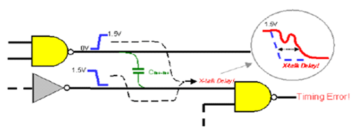
Capacitive crosstalk can induce noise (glitches) on a non-switching signal line routed with a switchable signal line, and can potentially cause functionality failures. Similarly, crosstalk can cause increased delays when an aggressor switches in the opposite direction of the victim. Conversely, an aggressor can cause decreased delays when switching in the same direction as the victim. This increase or decrease in delays can cause setup or hold time violations respectively, and may lead to reduced operating frequency and functional failures as shown in the figure 1.

Figure 1: capacitive coupling between two signal lines
Proposed Standard cell architecture
Signal integrity or capacitive crosstalk can be handled at each stage from pre-layout sizing to global/detail routing at SOC’s. Since capacitive crosstalk is routing dependent and coupling capacitance relies on the wire spacing and overlapping distance of the routes and interconnects, Hence crosstalk coupling can occur within any pair of adjacent signals, irrespective of whether they belong to the same logical/physical hierarchy or not. Therefore signal integrity issues can occur in below scenarios
- Between signals routed at SOC.
- Between Signals present at Hard IP blocks periphery to SOC top level routing.
- Between Standard cells routing and SOC signal routing.
In first two cases designer/integrator has sufficient design visibility and data available to analyze the crosstalk effects completely. However, in the third case chip integrator may not have visibility of sensitive signals present in standard cells, and similarly standard cells owner may not have idea about SOC’s environments in which cells are going to be placed. In proposed architecture of standard cells following below have been implemented to reduce the signal integrity issues
- Shielding critical nets within standard cells.
- Development of clock pins near ground power rail.
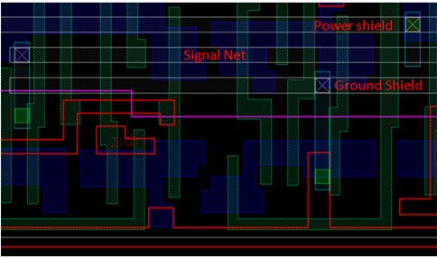
Shielding critical nets/signals with power lines is one of the technique for reducing the capacitive coupling which is implemented by adding VDD and VSS “shields” and sensitive signals being routed in between power lines as shown in figure1.

Figure 2: Shielding of critical net in standard cell
Power supply lines isolate critical signals, and in turn eliminate crosstalk effects that might have been occurred by adjacent wire transitions routed at SOC. Shielding critical net in standard cells will add accuracy of all functional and timing specs that an integrator might have during the course of global/detail routing at SOC.
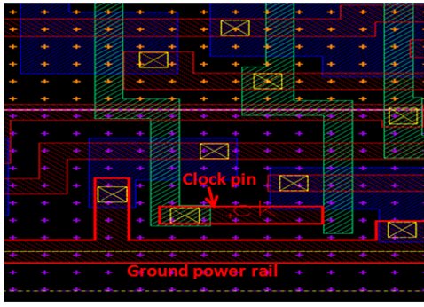
Clock signals are being one of most noise sensitive and critical signals from design point of view. There are numerous approaches that have been used across SOC’s to meet correct functional and timing requirements of clocks nets e.g. by routing clock signals with single width double spacing or double width double spacing. In proposed architectural solution shown in figure 2 cell clock pin is being created next to ground supply rail, such that clock pin is shielded with ground line from one side. Since development of clock pin is using Metal 1 and there is no other higher metal is used in horizontal and vertical routing direction near clock pin to give integrator freedom of routing clock pins with the different schemes as discussed in [2].

Figure 3: Development of clock pin near power supply rail
Conclusion:
In DSM technologies signal Integrity issues are potential sources of noise and design failure. Since signal integrity issues are hard to detect when occurs between standard cell route and signal route at SOC. Shielding of critical nets and keeping clock pins near ground power rails in standard cells will help to reduce signal integrity issues at SOC level.
References:
[1] Shyh Chyi Wong, “Modeling of interconnect capacitance, delay, and crosstalk in VLSI” IEEE Trans. Semiconductor Manufacturing, vol. 13 no. 1, pp. 108-111 FEB. 2000.
[2] Ravi Chhabra, Srijith Nair, Ekta Gujral “Understanding clock net routing with shrinking technology”
Authors:
Azeem Hasan: Working at Freescale Semiconductors, India as Senior Design Engineer and 4 years of experience in Physical Design, Analog Layout Design and Standard Cell Library Design.
Deepak Sharma: Working at Freescale Semiconductors, India as Lead Engineer and 8 years of experience in Physical Design, Analog Layout Design and Standard Cell Library Design.
Sachin Kalra: Working at Freescale Semiconductors, India as Senior Design Engineer and 6 years of experience in Physical Design, Analog Layout Design and Standard Cell Library Design.
Ajay Sharma: Working at Freescale Semiconductors, India as Lead Engineer and 8 years of experience in Physical Design, Analog Layout Design and Standard Cell Library Design.
Rahul Saxena: Working at Freescale Semiconductors, India as Principle Staff Design Engineer and 12 years of experience in Physical Design, Analog Layout Design and Standard Cell Library Design.
Related Semiconductor IP
- NPU IP Core for Mobile
- NPU IP Core for Edge
- Specialized Video Processing NPU IP
- HYPERBUS™ Memory Controller
- AV1 Video Encoder IP
Related White Papers
- SOC: Submicron Issues -> Deep signal integrity can be assured
- Signal Integrity --> Multipoint standard boosts LVDS
- Packaging concern: signal integrity issues rise with 500 Mbit/sec rates
- Signal Integrity --> LVDS extends utility of 1149.1 boundary scan test
Latest White Papers
- Ramping Up Open-Source RISC-V Cores: Assessing the Energy Efficiency of Superscalar, Out-of-Order Execution
- Transition Fixes in 3nm Multi-Voltage SoC Design
- CXL Topology-Aware and Expander-Driven Prefetching: Unlocking SSD Performance
- Breaking the Memory Bandwidth Boundary. GDDR7 IP Design Challenges & Solutions
- Automating NoC Design to Tackle Rising SoC Complexity