Clock Gate Logic Aware Design Closure
Ateet Mishra, Jatinder Kumar, Uchit Singhal (Freescale Semiconductors)
Silicon On Chip (SOC) consists of several logical gates connected to define some functionality. Timing Closure being a well known art to ensure that every single timing path between consecutive register will function properly. Timing Closure on an SOC defines the performance of a design. It involves lot of timing checks performed over sequential gates in the design, like setup hold timing etc.
Clock Gating which is a deliberate power saving phenomenon functions to save dynamic power consumption in an SOC. Similar to other sequential cells timing requirements are also required to be met on the clock gating cells. But being a part of clock tree latency clock gating latencies are usually lower than the other sequential elements which talks to enable the clock gating cells. This results in an overall negative skew in the timing requirement of these cells and sometimes proves to be a headache for an STA engineer.
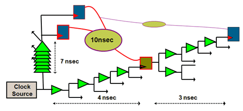
The clock gating checks often do not get the attention that they deserve early in the design cycle. Most of the EDA tools employed for CTS building deploy the clock gating cells as much close to the root as possible to save on dynamic power. This increases the amount of negative skew and lead to extra criticality in setup violations at the enable pin of that clock gating cell. Figure 1, shows the introduction of negative skews in case of clock gating setup checks after clock tree synthesis. The data path is shown in red color, where many start points are involved in triggering the clock gating enable for clock gating cell, and path will become setup critical as it has skew of 3nsec. Which will not be reflected till clock tree is built.

Figure 1
Consider the case in figure 1, While Placement and optimization, data path including flops and clock gating cells will be placed and optimize for 10 nsec. The timing path was just met till clock tree is built. But when Clock Tree is built, it introduces a Setup Violation of 3 nsec. In the conventional approach, to meet the design skew (to avoid hold) complete design is build at same latency. Also there is no control over latency of clock gating cells, as all clock gating cells are considered transparent.
Clock gate logic aware Design Closure
Our Paper describes a way to pro-actively shows the impact of clock tree building at the time of placement and optimization in the form of reduced latencies, and the approach shows more realistic violations on clock logic at synthesis or placement stage. That makes the placement & optimization process clock aware. Also it provide the necessary pull/push information for clock logic while clock tree building.
Clock Gate Aware Design Closure Algorithm follows:
- Based on the load on clock gating cells their negative latencies are calculated.
- With above information realistic placement and optimization is done.
- Final Decision on clock gating pull/push is decided based on timing violation on clock logic.
- Clock tree is build with the macro models generated by above analysis.
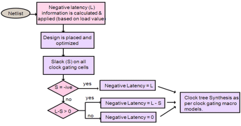
With above algorithm, our approach takes care of the mentioned situations in advance, at the time of placement, which makes best use of placement. And clock logic is optimized accurately at the early stage of design closure. Second part of the innovation guides the clock tree synthesis flow with the accurate latency of clock logic that will support easy closure of clock gating logic. The flowchart explaining the detailed steps is shown in figure 2.

Figure 2
The approach has two unique steps, first step ensures the correct level of placement and optimization of clock getting logic to meet required timing, while second step provide the expected latency for critical clock gating cells as macros to be considered while doing clock tree synthesis.

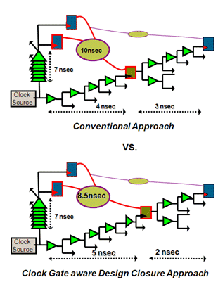
Figure 3
As shown in figure 3, the approach ‘clock gate aware design closure’ is able to deal with the clock gating timing closure. The intermediate steps are as below. The approach has proactively looked for the required post clock gating cell latency for clock, and information is passed while placement stage.
Step 1: Design is better optimized to 8.5 nsec.
Step 2: Information of pre clock gating and post clock gating latencies applied in clock tree helped maintaining a skew helping timing closure.
Conclusion
The explained approach is more specifically looks at the real post clock tree timing information of clock logic at placement stage, which enables best placement and optimization for clock logic. Also, seeing the timing slack it provides maximum latency of clock logic for better clock tree and hence timing results.
Related Semiconductor IP
- NPU IP Core for Mobile
- NPU IP Core for Edge
- Specialized Video Processing NPU IP
- HYPERBUS™ Memory Controller
- AV1 Video Encoder IP
Related White Papers
- Asynchronous Logic: large CMOS devices without a clock tree
- Low Power High Density Clock Gate
- Dynamically controlled logic gate design for all power modes
- Embedded Systems: Programmable Logic -> Common gateway networks enable remote programs
Latest White Papers
- Ramping Up Open-Source RISC-V Cores: Assessing the Energy Efficiency of Superscalar, Out-of-Order Execution
- Transition Fixes in 3nm Multi-Voltage SoC Design
- CXL Topology-Aware and Expander-Driven Prefetching: Unlocking SSD Performance
- Breaking the Memory Bandwidth Boundary. GDDR7 IP Design Challenges & Solutions
- Automating NoC Design to Tackle Rising SoC Complexity