Low Power High Density Clock Gate
Syed Shakir Iqbal, Nishant Madan, Mayank Tutwani (Freescale Semiconductors India Pvt. Ltd)
I – ABSTRACT
This paper presents a low power Clock Gating scheme for clock power improvement that reduces power dissipation by deactivating the clock signal to an inactive value (for clock gating cell) when clock is supposed to be gated (for soc). The presented circuit also overcomes the high clk-to-out delay of the conventional clock gating cell. It reduces the clk-to-out delay by reducing the number of inverter stages in clk-to-out path. Simulation results on 65nm technology show that the proposed approach improves power by at least 30% and reduces the clock-to-out by approximately 16% over the conventional clock gate architecture.
II - INTRODUCTION
As SoC designs continue to evolve with more features, so have the complexities and constraints leading towards a substantial increase in gate count. Low power, high density and performance have become a major challenge. Multiple techniques have been incorporated in designs for optimization in terms of power, area and performance. Clock gating is one such ubiquitous example capable of reducing dynamic power consumption significantly.
Due to extensive usage of clock gates the power dissipated by these gates themselves has turned out to be a major issue along with their area overhead. However, in order to save the dynamic power of the sequential elements the overhead posed by the clock gates themselves has a significant impact on the design.
III – CLOCK GATE
A clock gate is a standard design cell that receives the clock and a gating signal as an input and ensures that the clock propagates only when it’s required depending upon the gating signal. If the gating signal is synchronous with respect to the clock signal then a clock gate is nothing but a simple two input combinational AND/OR gate for positive/negative edge triggered registers respectively.
In most designs the implementation tool generally creates the gating signal using asynchronous inputs and hence in order to ensure a glitchless clock gating, a latch is inserted in the path of the gating signal before the AND/OR gate.
Two common topologies used for clock gating cells are AND-type clock gates and OR-type clock gates, which ensure glitchless clock propagation by gating the clock at low and high levels respectively. Figures 1(a) and 1(b) show the architecture standard integrated clock gating cell used widely in most SoCs. This cell is provided with two control signals enable (E/EB) and test enable (TE/TEB) and the input clock CP. The AND type clock gate is able to gate the propagation of high level of clock pulse while the OR type masks the low levels. Figure 2 shows the timing between these signals that ensures glitchless clock propagation.
The existing topology has an integrated negative D-latch and an AND gate. Though this design is simple and helps reduce dynamic power significantly, it is still debatable whether this is the most optimum clock gating structure.
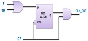
(a) AND type Clock Gate
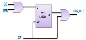
(b) OR type Clock Gate
Fig 1
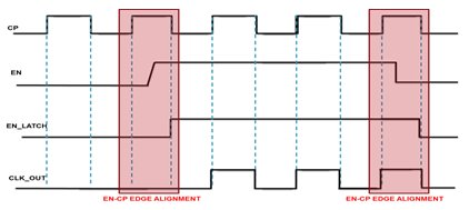
Fig 2: Glitchless clock switching in conventional clock gate.
In this paper we will discuss the issues associated with conventional clock gating circuits in terms the power, area and timing performance and based on these we propose an alternative architecture that will be a more optimal solution*.
IV – ISSUES IN CONVENTIONAL CLOCK GATES
Power saving is a key strategic advantage of using clock gates as they reduce idle dynamic power significantly. However, the current architecture only targets the clock gating for its loads.
The internal elements, specifically the latch clock inverters and NAND gate have uncontrolled clock toggling even during the idle stage. There is no self-gating mechanism provided within the clock gating cell that can help in reducing the idle dynamic power dissipation with it. It can be seen from figure 3 ,that in addition to the power dissipated by these clock gates themselves the clock path within the cell itself also comprises of multiple stages of combo-logic and thus may give rise to a significant clock-to-out delay which can impact timing as well.
Furthermore, in high performance designs it is very likely to have an intense usage of clock gates in the clock tree in order to reduce power as well as balance the clock loads.
This scenario then provides a challenge for the implementation team to ensure that clock gating not only reduces the dynamic power but also doesn’t impact the clock tree latency and skew significantly. For example, in 65nm if we have a SoC block being clocked at 750MHz(~1.33ns) , a clock gate with an average clock-to-out delay of ~300ps can significantly impact the clock tree and timing closure (22% of clock period eaten by clock gate).
Moreover, since the operating frequency is so high it will be a mandate for the designer to add clock gates more intensely in order to keep the power in check. However, at the same time intense usage of clock gates presents an overhead of extra leakage and dynamic power dissipation through these gates. These gates are often high drive strength cells in order to drive the multiple loads. With increased loads clock generating inverters inside CG cell keeps on burning the power as clock toggles on them always. Significant gain in power can be obtained if we can restrain this toggling factor.
Hence, in order to help the designers meet both the power as well as timing closures with least impact on silicon area we propose a new architecture of a self-gated, low power, high-density clock gate that overcomes the limitation of the conventional clock gating cell.

Fig 3: Conventional clock gate architecture
V – PROPOSED ARCHITECTURE
The proposed circuit is based on the concept of internal-clock-gating and hybrid combinational-sequential logic. The architecture basically aims at reducing the internal clock toggling power by generating a self-gating scheme that will gate the secondary clock inverter and clock-enable ANDing logic during the idle/stop clock propagation mode. The added advantage of this scheme is that it also reduces the clock-to-out path by merging the internal latch sequential loop and clock invertors in This new topology further, helps us in saving an area of equivalent to 2 inverters. Figure 4 shows the primary architecture of the proposed cell.
The operation is a hybrid of AND & OR gate type clock gates (AND type driving the external loads and OR type used for self-gating). By gating the internal clock when the Clock Gate is in idle state dynamic power consumption is reduced significantly. In addition, merging the combo logic that follows the latch within the latching loop a slight gain in area as well as reduced leakage power is also obtained from this topology.

Fig 4: Primary architecture of proposed clock gate
The basic idea behind using this circuit is that we only wish to use the latch for latching a ‘1’ via the feedback loop. However, this presents us with the issue that the internal clock gating signal CEN attains value depending on the state of CPN & CP and the CPN itself is generated from CP and CEN.
A race condition may exist when both CP and CPN are high and EN makes a 0-1 transition. This can allow a false passage of a weak 1 in the latch which may produce a glitch in internal gated clock CPN and hence the output Q if the feedback PMOS is too sluggish.
Furthermore, when enable is low for a long time and CP is high, the zero at node CEN is not latched for half cycle. The timing diagram in figure 5 shows when this type of scenario may present an issue.

Fig 5 Timing issues for not latching a “0” in clock gate
To eliminate these kind of scenarios we came up with a new circuit topology where by merging the Transmission gate within the NOT/NOR the race condition is avoided as EN cannot make a 0-1 transition during CP high. Also by adding two new NMOS for feedback for latching a Zero is ensured for all CP = 1 as depicted in below circuit topology figure 6.
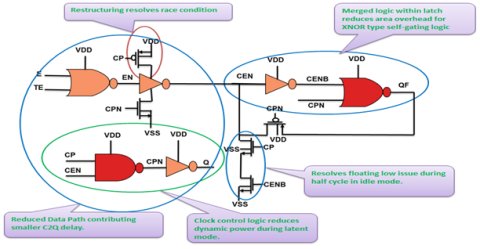
Fig 6 Improved architecture to resolve timing issues.
Table 1 show that the proposed architecture has the exact same truth table as that of the conventional clock gating cell. It can be seen from the timing diagram in figure 7 shows how the new topology resolves the above floating and race condition scenarios efficiently with degrading the timing parameters.

TABLE 1: Excitation table comparison of prior art and modified proposed topology
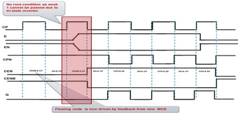
Fig 7: Glitchless clock gating in proposed clock gate
VI – CONCLUSION AND RESULTS
The simulation results for the proposed architecture for 65nm technology show that the proposed scheme not only helps reduce the overall power dissipation of the cell but also provides a slight improvement in terms of timing. Figure 8 is a sample simulation snapshot which shows how the internal self gating is enabled within the proposed clock gate while ensuring no glitches at the output clock waveform.
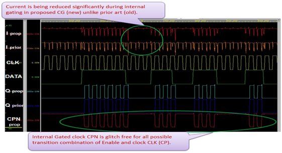
Fig 8 Simulation snapshot for proposed clock gate
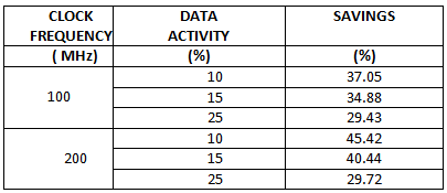
TABLE 2: Power savings in proposed topology w.r.t. conventional architecture

TABLE 3: Timing improvements in proposed topology w.r.t. conventional architecture
SOC Level Results:
- CG cell contribution to sequential elements [CG Count / (CG + FLOP count) ] = 3.74%
- Clock gate power contribution :
- CG cell contribution to total sequential power = 6.17%
- CG cell contribution to total power = 0.12%
- Clock gate enable activity = 4%
- This lower activity signifies that in our current 65nm SoCs working at a frequency range (~160-250) most efficient power savings can be obtained from the proposed art instead of XNOR-CG without impacting the timing or area significantly.

Table 4: Overall comparison between conventional and proposed architecture
Related Semiconductor IP
- NFC wireless interface supporting ISO14443 A and B with EEPROM on SMIC 180nm
- DDR5 MRDIMM PHY and Controller
- RVA23, Multi-cluster, Hypervisor and Android
- CXL 3.0 Controller
- ECC7 Elliptic Curve Processor for Prime NIST Curves
Related White Papers
- A High Density, High Performance, Low Power Level Shifter
- High Density - Low power Flip-Flop
- Clock domain modeling is essential in high density SoC design
- A Clock Tree Synthesis Flow Tailored for Low Power
Latest White Papers
- TROJAN-GUARD: Hardware Trojans Detection Using GNN in RTL Designs
- How a Standardized Approach Can Accelerate Development of Safety and Security in Automotive Imaging Systems
- SV-LLM: An Agentic Approach for SoC Security Verification using Large Language Models
- Enabling Chiplet Design Through Automation and Integration Solutions
- Shift-Left Verification: Why Early Reliability Checks Matter