Analysis of RDC Paths for a million gate SoC
Ankush Sethi, Freescale Semiconductor India Pvt Ltd
Abstract
Reset is necessary to initialize the system and reach to a known state. Just like multiple clocks are required in an SoC to sustain various use models and performance, multiple resets are designed to cater different functional requirements. With this advent we also invite some issues due to crossings among different reset domains. In a sequential design, if the reset of source register is different from the reset of destination register even though the data path is in same clock domain, this will become asynchronous crossing path and can cause metastability at destination register. This is being termed as Reset Domain Crossing (RDC). Some linting and CDC tools detect RDC issues. But the tool throws a lot of violations as it is blindly looking for violating structures. This paper discusses how to analyze and waive/fix RDC paths once flagged by tool.
1. Introduction
First question that arises in mind is the need of multiple resets?
In most of the SoCs, we have multi phase reset sequence requirement e.g. before the initialization (de-assertion of reset) of core it is required that the device flash is initialized. In this case we need to design different resets for the flash and the core. There is certain information that the user would like to have after coming out of warm/functional reset e.g. the value of status registers which captures the event causing functional reset. So we need to keep those registers at POR (Power on Reset). Also whenever software requests a warm/functional to the system the contents of the System RAM are expected to retain its value. Hence we need to have a reset different from warm reset for the System RAM also. In some of the cases requirement of different resets is application driven. For instance there may be some time keeping functionality like RTC that is required to work until POR (Power on Reset) is asserted. Also we may require certain secure blocks to retain their value in case of warm/functional reset.
2. Analysis of RDC paths
2.1 Identifying False Violations
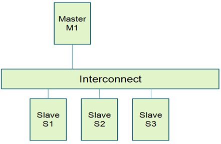
Every tool must have the capability to filter out false violations based on reset ordering as RDC issues occur only when assertion of reset of source flop doesn’t cause assertion of reset of destination flop. But there may be cases where structurally there is a problem but there is no issue functionally. One such case is discussed here (Fig 1). In this design, we have Master M1 working at functional reset and some registers in slave S2 working at POR (Power on Reset). Here we will have a RDC violating path from flops of M1 to registers of S2 through Interconnect combinational logic (e.g. write data mux). However, if we know by design that M1 will never be accessing registers of S2 then we may safely ignore this false path.

Fig 1: Identifying False Violations
2.2 Meeting Timing Parameters
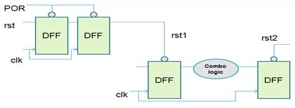
We can waive RDC paths if we are meeting reset assertion timing for them. The tool will however show the violation as there is a problem structurally. In Fig 2, we meet timing parameters for path from “assertion of reset rst1” to “D input of the destination flop”. Here there is a prerequisite that rst1 is launched on the same clock as that of source and destination flops. If this is not the case then we need to add synchronizers (whose reset will be POR) to achieve this as shown in fig below. Also it needs that Reset Q timing arc for the source flop is enabled.

Fig 2: Meeting timing parameters
2.3 Custom Synchronization/Handshake
There are many cases where we fix RDC violations by adding some custom synchronization or handshake mechanism. But the tool may not be able to identify such structures and will flag them as violations even if it is known that there won’t be any metastability propagation in design in such cases. Two such cases are discussed below:
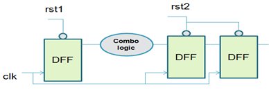
a) In most of the design, we use another sync flop at fan out of destination flop (Fig 3(a)). This ensures that metastability occurring at destination flop is blocked from propagating into design. However this circuitry adds additional single cycle latency so the designer must carefully review the paths before adding it.

Fig 3(a): Synchronizing destination output
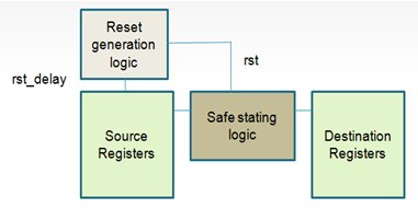
b) The above described scheme may not be sufficient to handle all the RDC violating paths. The designer may device certain custom circuits to prevent metastability at destination flop. In the below design (Fig 3(b)), we have inserted a safe stating logic in the path of destination registers. Whenever a reset request is there, the Reset generation logic generates a reset signal “rst” for the Safe stating logic to detect that the source register is going to reset in next two or three cycles (through signal rst_delay). The Safe stating logic gates the input of destination registers. Thus preventing those from getting metastable when the reset of source flop “rst_delay” asserts.

Fig 3(b): Safe stating the destination
3. Summary
The paper discusses how to waive and fix RDC violations once flagged by tool. It becomes necessary to analyze these violations early in design cycle to avoid any ECO or silicon re – spin. However the designer must analyze the conditions under which the proposed solutions can be used.
Related Semiconductor IP
- NPU IP Core for Mobile
- NPU IP Core for Edge
- Specialized Video Processing NPU IP
- HYPERBUS™ Memory Controller
- AV1 Video Encoder IP
Related White Papers
- Efficient analysis of CDC violations in a million gate SoC, part 1
- Efficient analysis of CDC violations in a million gate SoC, part 2
- UPF Constraint coding for SoC - A Case Study
- Performance Evaluation of machine learning algorithms for cyber threat analysis SDN dataset
Latest White Papers
- Ramping Up Open-Source RISC-V Cores: Assessing the Energy Efficiency of Superscalar, Out-of-Order Execution
- Transition Fixes in 3nm Multi-Voltage SoC Design
- CXL Topology-Aware and Expander-Driven Prefetching: Unlocking SSD Performance
- Breaking the Memory Bandwidth Boundary. GDDR7 IP Design Challenges & Solutions
- Automating NoC Design to Tackle Rising SoC Complexity