A Design of System on a Chip for Voice over Wireless LAN
Hun-sik Kang, In-ki Hwang, Chan-won Park, Gi-jong Koo, Jae-ho Lee, Jung-hak Kim, Woon-seob So,
Daeho-Kim, Do-young Kim, Jung-sik Kim
VoIP Terminal Technology Team, BcN Service Research Group, ETRI
161, Gajeong-dong, Yuseong-gu, Daejeon, KOREA
Abstract :
VoIP SoC(System on a Chip) over wireless LAN is presented, which integrates u-processor, wireless access block, several user interfaces and voice signal interfaces. VoIP system over wireless can be easily implemented with a low cost, less complexity. To support priority issues of voice signal, dual queuing strategy is adopted. It also provides WLAN-PHY which supports high speed data access up to 24MHz using OFDM-based baseband modem.. Its functionality can be verified with test modes integrated. VoIP SoC over WLAN is fabricated in 0.18um cmos process technology and operates in 1.8V for core logic, 3.3V for I/O logic. The logic gate counts amounts to approximately 2.1 millions and many number of macros including memory is used. Its package is BGA with 312 pins and size of 27mm x 27mm.
1. Introduction
Over the past a few years, several communication services using WLAN (Wireless Local Area Network) are increasing. As a result, wireless local data networks are gaining the momentum and making their way into residential, commercial, industrial and public areas [1]. These trends are more and more accelerated in the place like airports, hotels and coffee shops, which typically have a many floating end users. In addition, since wireless connections provide more flexible network configuration and access with a low cost, use of WLAN is now on the increase in university campuses and conference. While the majority of traffic in WLAN deployment is centralized on data communications such as e-mail, web browsing and internet, voice over WLAN is being popular as Voice over IP (VoIP) applications flourish.
To develop VoWLAN (Voice over WLAN) system shown in figure 1, various discrete component, for example u-processor, wireless MAC, wireless PHY, key pad , LCD controller and other user interface logic, audio interface, will be required. Therefore, complexity and cost of system are increased in case of making VoWLAN system with each component needed. To overcome these problems, SoC which integrates a number of components or modules into a single chip is indispensable to make voice communications using WLAN spread in our life and can also make time earlier.
This paper presents design and architecture of a single chip or SoC for providing VoIP services over the wireless local area network. Firstly, necessity of SoC, wide spread use of WLAN and advent of VoIP are described in introduction. And then, chapter 2 gives a general description on the architecture of implemented SoC and the detailed explanation of principal blocks. Chapter 3 discusses information of design and a brief description of test. And finally, in section 4, the conclusion will be reached.
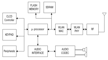
Fig 1. Wireless VoIP system
2. Chip Architecture
2.1 General Descriptions
Architecture of SoC is designed with module-based approach and basis of IP(Intellectual Property) blocks for design-reuse and expandability. In addition, it has so bus-oriented that it can be changed with ease. SoC consists of four principal parts which are process core, voice signal interface block, wireless access block and user interface logic. Each of the main blocks is all connected to ARM AMBA [2] bus with data and address of 32bits. Fig 2 shows the overall architecture of SoC. Processor core is comprised of ARM926EJ-S RISC processor, DMAC (Direct Memory Access Controller), bus bridge, I/O decoder and clock/reset generation logic. Voice signal interface logic has PCM (Pulse Coded Modulation) interface which can process the 8 or 16 bits of PCM data.
And it also has TDM (Time Division Multiplexing) for connecting and interfacing with signals from PSTN (Public Switched Telephone Network). To make voice communication possible, signals through these voice interface logics is processed with the several software routines like narrow band/wide band codec, G.711, G.723 [3][4], de-jittering, echo-cancellation. Wireless access block is composed of wireless MAC and PHY. Wireless MAC has the functionality of DCF and dual queue structure to support QoS. Wireless PHY is a OFDM based base-band processor which is compatible with IEEE 802.11a. There are a few components to facilitate user interface. Each of them is as follows. Two UARTs for IrDA and debug, 32 GPIO(General Purpose Input Output) for test logic and other purposes, SCI(Smart Card Interface), SSP (Synchronous Serial Port), and CLCD for video phone.
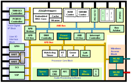
Fig 2. Architecture of wireless VoIP SoC
2.2 Processor Core Block
As an processor for SoC, ARM926EJ-S [5][6] with built-in DSP features is selected not to use DSP which occupies a large portion of chip. Operating speed of processor is 200MHz and operating frequency of AHB (Advanced High-performance Bus) and APB (Advanced Peripheral Bus) is a half speed of processor, to say 100MHz. interfaces with AMBA can be achieved with address and data bus of 32bits. To sustain the external memory bandwidth, flash and synchronous memory controller is connected to AHB. Also located on AHB are a bridge to the lower bandwidth APB, DMA controller, CLCD (Color LCD Controller) and I/O decoder. Several kinds of peripheral devices such as UART, GPIO and WLAN devices are connected to advanced peripheral bus.
To support external memory interface, there are two memory controllers, each of them is static memory controller, SDRAM controller. SMC (Static Memory Controller) exists for flash memory. SMC includes the various features which are asynchronous page mode, extended wait, and programmable wait states. SDRAM controller has four chip selects and is able to control clock to the external memory devices to save the power. Other interface logic to share the pads of memory controller is provided.
VIC (Vector Interrupt Controller) provides 16 vectored interrupts to handle the interrupts by the different interrupt sources. Its priority can be updated by setting the interrupt address register. VIC provides also fast interrupt request for fast, low latency interrupt handling.
DMAC (Direct Memory Access Controller) supports a maximum of 16 channels, incrementing or non-incrementing addressing, and 8/16/32-bit wide transactions. Four of 16 channels exist for external devices, the rest of them for internal purpose. And also a specific hardware priority is given to the each channel of DMA. If request from two channels become active at the same time, channel with the highest priority is serviced first.
Besides the above-mentioned components, system controller, watch dog timer and real clock timer are included. System controller provides control of system operation modes, clock control and status, definitions of system response of interrupts, capturing the reset status and soft reset generation. Watch dog timer consists of a 32bit down counter with a programmable timeout interval that has the capability to generate an interrupt and a reset signal on timing out. It is used to generate a reset signal to SoC when software failure occurred.
2.3 WLAN Access Block
Wireless access block consists of a wireless MAC [7][8] that controls the access to the medium and mediates collisions, a wireless PHY which gives digital signal processing, modulation and decoding the received signal from wireless medium.
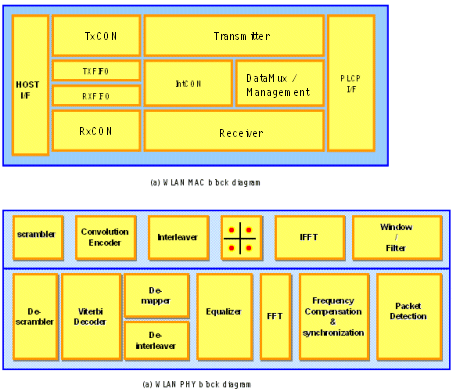
Fig 3. Structures of WMAC/WPHY
WMAC (Wireless MAC) are comprised with host interface logic located on AMBA 32bits bus, transmit and receive controller, two transmit/receive FIFO to buffer sending and receiving data, logic to manage the RF system and WPHY, and PLCP interface logic. WMAC adopts dual queuing strategy to support QoS for voice signals [9]. WPHY is OFDM-based signal processing block in accordance with IEEE 802.11a [10]. It provides data rates up to 24Mbps. Fig 3 shows the structure of WLAN MAC and WPHY.
2.4 Voice Signal Interface and User Interface Block
Pulse coded modulated voice signal of 8 or 16 bits is connected to processor through the PCM interface module. For narrow band codec, it is sampled by 8 KHz for narrow band codec and by 16KHz for wide band codec. TDM bus controllers, which is for connection to the PSTN, supports external interface to 4 channels. It is clocked with 2.048 MHz and generates frame sync signal of 8 KHz.
2.5 Clock Generation and System Control
The structure of clock generation logic is shown in figure 4. Reference clock signal of 40 MHz is connected to input of PLL, which generates 200 MHz clock for system. Clock frequency of PLL can be controlled by system controller. Input clocks to the each block of SoC are separated into two categories. One is for the peripheral blocks which is asynchronous with processor or AMBA bus. Therefore, it is generated by clock generator which divides output of PLL with values of clock control registers in system controller. The other is for the blocks which is synchronous with system bus. Its clock frequency is also changeable by system controller. There are four operation modes in SoC, each of which is SLEEP, DOZE, SLOW, NORMAL. In SLEEP mode, clocks to the processor and system bus are disabled. System controller clock is driven from a slow speed oscillator (32 KHz) in this mode. When an interrupt is activated through the VIC, system moves into the DOZE mode. All blocks in SoC operate with low frequency oscillator (32 MHz) in DOZE mode. In SLOW mode, both the system clocks and the system controller clocks are driven from the output of the crystal oscillator of 40 MHz.
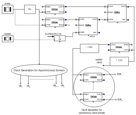
Figure 4. Structure of clock generations
3. Design Summary
Figure 5 shows the design flow and tools used in each step to implement wireless VoIP SoC. In system design of wireless PHY, SPW(Signal Processing Workbench) and MATLAB is used to verify the system model. Co-verification between models of hardware and software is done through the Seamless CVE tool.
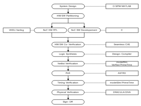
Fig. 5. Design flow and tools for wireless VoIP SoC
Table 1 shows chip specific information including logic gate counts, system clock, numbers of macros and so on. The equivalent logic gate counts amounts to approximately 2.1 millions. (calculated by 2 input NAND gate as one) The implemented SoC is fabricated with 0.18 um CMOS process of TSMC. A 1.8V for core (3.3V I/O) and BGA package of 316 pins are used.
Table 1. SoC-specific Information
Figure 5 shows the layout view of wireless VoIP SoC. PLL and clock generation logic can be found at the top of left side. At the middle of left side, ARM926EJ-S processor can be seen. On the top and bottom of processor, TCM(Tightly Coupled Memory) is located. TCMs are intended for storing real-time and performance critical code. As a result, they should be located in the proximate place of processor. Standard cells are scattered over the most of right side. Macros such as memories can be seen in the outer ring of right side.
Test modes of SoC can be divided into four main parts: test for functionality of each principal block, PLL-bypass (tested by external master clock), test of PLL and processor by setting the test pins externally, loop back test. Each of main block can be verified in connection with processor through the primary inputs and outputs of chip. It has the registers to control and support test of block. If these registers can be configured accordingly through the processor, functionality of main block can be verified through chip pins. Loop back test is intended for verifying the function of path from voice to wireless access block.
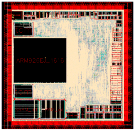
Figure 6. Layout view of implemented SoC.
4. Conclusions
This paper described the architecture and design on the SoC for wireless voice over IP. The implemented SoC is intended for providing the VoIP system on wireless medium with less complexity and low cost. Because it is also designed with modular-base approach and bus oriented architecture, it helps us to expand system more easily and design reuse. The wireless VoIP SoC is fabricated with a 0.18 um CMOS process and 1.8/3.3V operation in TSMC. It uses ARM926EJ-S as an embedded processor and operates at 200 MHz. It is run on the Linux operating system embedded. It also support several test modes so that its functional operation can be verified through primary input/outputs. Using this SoC can make the system for VoIP applications with ease and at a reduced cost.
References:
[1] Ashutosh Dutta, Prathima Agrawal, “Voice Performace in WLAN Networks – An Experimental Study” GLOBECOM ’03, IEEE, Volume:6, 1-5 Dec. 2003.
[2] ARM “AMBATM Specification (Rev 2.0)”, 1999.
[3] ITU-T Recommendation G.711, "Pulse Code Modulation (PCM) of Voice Frequencies", 1989.
[4] ITU-T Recommendation G.723.1, "Dual Rate Speech Coder for Multimedia Communications Transmitting at 5.3 and 6.3kbps ", 1996.
[5] ARM, “ARM926EJ-S (Rev 0) Technical Reference Manual”, 2002.
[6] ARM, “ARM926EJ_1616 Revision:r0p4, Integration Manual” 2003.IETF Recommendation H.248(06/2000), Gateway Control Protocol.
[7] IEEE 802.11 (1999), Wireless LAN Media Access Control(MAC).
[8] IEEE 802.11e (2004), Media Access Control(MAC) Quality of Service(QoS) Enhancements.
[9] Jeonggyun Yu, Sunghyun Choi, Jaehwan Lee, “Enhancement of VoIP over IEEE 802.11 WLAN via Dual Queue Strategy”, 2004 IEEE International Conference on Communications, Volume: 6, 20-24 June 2004: p. 3706-3711.
[10] IEEE Std 802.11a/D7.0-1999, Part 11, “Wireless LAN Medium Access Control (MAC) and Physical Layer (PHY) Specifications: High Speed Physical Layer in the 5GHz Band..
Daeho-Kim, Do-young Kim, Jung-sik Kim
VoIP Terminal Technology Team, BcN Service Research Group, ETRI
161, Gajeong-dong, Yuseong-gu, Daejeon, KOREA
Abstract :
VoIP SoC(System on a Chip) over wireless LAN is presented, which integrates u-processor, wireless access block, several user interfaces and voice signal interfaces. VoIP system over wireless can be easily implemented with a low cost, less complexity. To support priority issues of voice signal, dual queuing strategy is adopted. It also provides WLAN-PHY which supports high speed data access up to 24MHz using OFDM-based baseband modem.. Its functionality can be verified with test modes integrated. VoIP SoC over WLAN is fabricated in 0.18um cmos process technology and operates in 1.8V for core logic, 3.3V for I/O logic. The logic gate counts amounts to approximately 2.1 millions and many number of macros including memory is used. Its package is BGA with 312 pins and size of 27mm x 27mm.
1. Introduction
Over the past a few years, several communication services using WLAN (Wireless Local Area Network) are increasing. As a result, wireless local data networks are gaining the momentum and making their way into residential, commercial, industrial and public areas [1]. These trends are more and more accelerated in the place like airports, hotels and coffee shops, which typically have a many floating end users. In addition, since wireless connections provide more flexible network configuration and access with a low cost, use of WLAN is now on the increase in university campuses and conference. While the majority of traffic in WLAN deployment is centralized on data communications such as e-mail, web browsing and internet, voice over WLAN is being popular as Voice over IP (VoIP) applications flourish.
To develop VoWLAN (Voice over WLAN) system shown in figure 1, various discrete component, for example u-processor, wireless MAC, wireless PHY, key pad , LCD controller and other user interface logic, audio interface, will be required. Therefore, complexity and cost of system are increased in case of making VoWLAN system with each component needed. To overcome these problems, SoC which integrates a number of components or modules into a single chip is indispensable to make voice communications using WLAN spread in our life and can also make time earlier.
This paper presents design and architecture of a single chip or SoC for providing VoIP services over the wireless local area network. Firstly, necessity of SoC, wide spread use of WLAN and advent of VoIP are described in introduction. And then, chapter 2 gives a general description on the architecture of implemented SoC and the detailed explanation of principal blocks. Chapter 3 discusses information of design and a brief description of test. And finally, in section 4, the conclusion will be reached.

Fig 1. Wireless VoIP system
2. Chip Architecture
2.1 General Descriptions
Architecture of SoC is designed with module-based approach and basis of IP(Intellectual Property) blocks for design-reuse and expandability. In addition, it has so bus-oriented that it can be changed with ease. SoC consists of four principal parts which are process core, voice signal interface block, wireless access block and user interface logic. Each of the main blocks is all connected to ARM AMBA [2] bus with data and address of 32bits. Fig 2 shows the overall architecture of SoC. Processor core is comprised of ARM926EJ-S RISC processor, DMAC (Direct Memory Access Controller), bus bridge, I/O decoder and clock/reset generation logic. Voice signal interface logic has PCM (Pulse Coded Modulation) interface which can process the 8 or 16 bits of PCM data.
And it also has TDM (Time Division Multiplexing) for connecting and interfacing with signals from PSTN (Public Switched Telephone Network). To make voice communication possible, signals through these voice interface logics is processed with the several software routines like narrow band/wide band codec, G.711, G.723 [3][4], de-jittering, echo-cancellation. Wireless access block is composed of wireless MAC and PHY. Wireless MAC has the functionality of DCF and dual queue structure to support QoS. Wireless PHY is a OFDM based base-band processor which is compatible with IEEE 802.11a. There are a few components to facilitate user interface. Each of them is as follows. Two UARTs for IrDA and debug, 32 GPIO(General Purpose Input Output) for test logic and other purposes, SCI(Smart Card Interface), SSP (Synchronous Serial Port), and CLCD for video phone.

Fig 2. Architecture of wireless VoIP SoC
2.2 Processor Core Block
As an processor for SoC, ARM926EJ-S [5][6] with built-in DSP features is selected not to use DSP which occupies a large portion of chip. Operating speed of processor is 200MHz and operating frequency of AHB (Advanced High-performance Bus) and APB (Advanced Peripheral Bus) is a half speed of processor, to say 100MHz. interfaces with AMBA can be achieved with address and data bus of 32bits. To sustain the external memory bandwidth, flash and synchronous memory controller is connected to AHB. Also located on AHB are a bridge to the lower bandwidth APB, DMA controller, CLCD (Color LCD Controller) and I/O decoder. Several kinds of peripheral devices such as UART, GPIO and WLAN devices are connected to advanced peripheral bus.
To support external memory interface, there are two memory controllers, each of them is static memory controller, SDRAM controller. SMC (Static Memory Controller) exists for flash memory. SMC includes the various features which are asynchronous page mode, extended wait, and programmable wait states. SDRAM controller has four chip selects and is able to control clock to the external memory devices to save the power. Other interface logic to share the pads of memory controller is provided.
VIC (Vector Interrupt Controller) provides 16 vectored interrupts to handle the interrupts by the different interrupt sources. Its priority can be updated by setting the interrupt address register. VIC provides also fast interrupt request for fast, low latency interrupt handling.
DMAC (Direct Memory Access Controller) supports a maximum of 16 channels, incrementing or non-incrementing addressing, and 8/16/32-bit wide transactions. Four of 16 channels exist for external devices, the rest of them for internal purpose. And also a specific hardware priority is given to the each channel of DMA. If request from two channels become active at the same time, channel with the highest priority is serviced first.
Besides the above-mentioned components, system controller, watch dog timer and real clock timer are included. System controller provides control of system operation modes, clock control and status, definitions of system response of interrupts, capturing the reset status and soft reset generation. Watch dog timer consists of a 32bit down counter with a programmable timeout interval that has the capability to generate an interrupt and a reset signal on timing out. It is used to generate a reset signal to SoC when software failure occurred.
2.3 WLAN Access Block
Wireless access block consists of a wireless MAC [7][8] that controls the access to the medium and mediates collisions, a wireless PHY which gives digital signal processing, modulation and decoding the received signal from wireless medium.

Fig 3. Structures of WMAC/WPHY
WMAC (Wireless MAC) are comprised with host interface logic located on AMBA 32bits bus, transmit and receive controller, two transmit/receive FIFO to buffer sending and receiving data, logic to manage the RF system and WPHY, and PLCP interface logic. WMAC adopts dual queuing strategy to support QoS for voice signals [9]. WPHY is OFDM-based signal processing block in accordance with IEEE 802.11a [10]. It provides data rates up to 24Mbps. Fig 3 shows the structure of WLAN MAC and WPHY.
2.4 Voice Signal Interface and User Interface Block
Pulse coded modulated voice signal of 8 or 16 bits is connected to processor through the PCM interface module. For narrow band codec, it is sampled by 8 KHz for narrow band codec and by 16KHz for wide band codec. TDM bus controllers, which is for connection to the PSTN, supports external interface to 4 channels. It is clocked with 2.048 MHz and generates frame sync signal of 8 KHz.
2.5 Clock Generation and System Control
The structure of clock generation logic is shown in figure 4. Reference clock signal of 40 MHz is connected to input of PLL, which generates 200 MHz clock for system. Clock frequency of PLL can be controlled by system controller. Input clocks to the each block of SoC are separated into two categories. One is for the peripheral blocks which is asynchronous with processor or AMBA bus. Therefore, it is generated by clock generator which divides output of PLL with values of clock control registers in system controller. The other is for the blocks which is synchronous with system bus. Its clock frequency is also changeable by system controller. There are four operation modes in SoC, each of which is SLEEP, DOZE, SLOW, NORMAL. In SLEEP mode, clocks to the processor and system bus are disabled. System controller clock is driven from a slow speed oscillator (32 KHz) in this mode. When an interrupt is activated through the VIC, system moves into the DOZE mode. All blocks in SoC operate with low frequency oscillator (32 MHz) in DOZE mode. In SLOW mode, both the system clocks and the system controller clocks are driven from the output of the crystal oscillator of 40 MHz.

Figure 4. Structure of clock generations
3. Design Summary
Figure 5 shows the design flow and tools used in each step to implement wireless VoIP SoC. In system design of wireless PHY, SPW(Signal Processing Workbench) and MATLAB is used to verify the system model. Co-verification between models of hardware and software is done through the Seamless CVE tool.

Fig. 5. Design flow and tools for wireless VoIP SoC
Table 1 shows chip specific information including logic gate counts, system clock, numbers of macros and so on. The equivalent logic gate counts amounts to approximately 2.1 millions. (calculated by 2 input NAND gate as one) The implemented SoC is fabricated with 0.18 um CMOS process of TSMC. A 1.8V for core (3.3V I/O) and BGA package of 316 pins are used.
Table 1. SoC-specific Information
| System Clock | 200MHz |
| HDL used | Verilog/VHDL |
| Logic Gate Counts | 2.1 millions |
| macros | 31 macros |
| memory | ~1Mbytes (including ~12Kbytes ROM) |
| processor | ARM926EJ-S |
| Process/Voltage | 0.18um/1.8V(core)/3.3V(IO) |
| Package | 316 pin BGA(27mmX27mm) |
Figure 5 shows the layout view of wireless VoIP SoC. PLL and clock generation logic can be found at the top of left side. At the middle of left side, ARM926EJ-S processor can be seen. On the top and bottom of processor, TCM(Tightly Coupled Memory) is located. TCMs are intended for storing real-time and performance critical code. As a result, they should be located in the proximate place of processor. Standard cells are scattered over the most of right side. Macros such as memories can be seen in the outer ring of right side.
Test modes of SoC can be divided into four main parts: test for functionality of each principal block, PLL-bypass (tested by external master clock), test of PLL and processor by setting the test pins externally, loop back test. Each of main block can be verified in connection with processor through the primary inputs and outputs of chip. It has the registers to control and support test of block. If these registers can be configured accordingly through the processor, functionality of main block can be verified through chip pins. Loop back test is intended for verifying the function of path from voice to wireless access block.

Figure 6. Layout view of implemented SoC.
4. Conclusions
This paper described the architecture and design on the SoC for wireless voice over IP. The implemented SoC is intended for providing the VoIP system on wireless medium with less complexity and low cost. Because it is also designed with modular-base approach and bus oriented architecture, it helps us to expand system more easily and design reuse. The wireless VoIP SoC is fabricated with a 0.18 um CMOS process and 1.8/3.3V operation in TSMC. It uses ARM926EJ-S as an embedded processor and operates at 200 MHz. It is run on the Linux operating system embedded. It also support several test modes so that its functional operation can be verified through primary input/outputs. Using this SoC can make the system for VoIP applications with ease and at a reduced cost.
References:
[1] Ashutosh Dutta, Prathima Agrawal, “Voice Performace in WLAN Networks – An Experimental Study” GLOBECOM ’03, IEEE, Volume:6, 1-5 Dec. 2003.
[2] ARM “AMBATM Specification (Rev 2.0)”, 1999.
[3] ITU-T Recommendation G.711, "Pulse Code Modulation (PCM) of Voice Frequencies", 1989.
[4] ITU-T Recommendation G.723.1, "Dual Rate Speech Coder for Multimedia Communications Transmitting at 5.3 and 6.3kbps ", 1996.
[5] ARM, “ARM926EJ-S (Rev 0) Technical Reference Manual”, 2002.
[6] ARM, “ARM926EJ_1616 Revision:r0p4, Integration Manual” 2003.IETF Recommendation H.248(06/2000), Gateway Control Protocol.
[7] IEEE 802.11 (1999), Wireless LAN Media Access Control(MAC).
[8] IEEE 802.11e (2004), Media Access Control(MAC) Quality of Service(QoS) Enhancements.
[9] Jeonggyun Yu, Sunghyun Choi, Jaehwan Lee, “Enhancement of VoIP over IEEE 802.11 WLAN via Dual Queue Strategy”, 2004 IEEE International Conference on Communications, Volume: 6, 20-24 June 2004: p. 3706-3711.
[10] IEEE Std 802.11a/D7.0-1999, Part 11, “Wireless LAN Medium Access Control (MAC) and Physical Layer (PHY) Specifications: High Speed Physical Layer in the 5GHz Band..
Related Semiconductor IP
- 8MHz / 40MHz Pierce Oscillator - X-FAB XT018-0.18µm
- UCIe RX Interface
- Very Low Latency BCH Codec
- 5G-NTN Modem IP for Satellite User Terminals
- 400G UDP/IP Hardware Protocol Stack
Related Articles
- Customizing a Large Language Model for VHDL Design of High-Performance Microprocessors
- Design and implementation of a hardened cryptographic coprocessor for a RISC-V 128-bit core
- A Survey on the Design, Detection, and Prevention of Pre-Silicon Hardware Trojans
- CANDoSA: A Hardware Performance Counter-Based Intrusion Detection System for DoS Attacks on Automotive CAN bus
Latest Articles
- SNAP-V: A RISC-V SoC with Configurable Neuromorphic Acceleration for Small-Scale Spiking Neural Networks
- An FPGA Implementation of Displacement Vector Search for Intra Pattern Copy in JPEG XS
- A Persistent-State Dataflow Accelerator for Memory-Bound Linear Attention Decode on FPGA
- VMXDOTP: A RISC-V Vector ISA Extension for Efficient Microscaling (MX) Format Acceleration
- PDF: PUF-based DNN Fingerprinting for Knowledge Distillation Traceability