40G UCIe IP Advantages for AI Applications
By Aparna Tarde, Manuel Mota (Synopsys)
The deployment of generative AI in the devices we use every day is growing, driving demand for large language model sizes and higher compute performance. According to a presentation by Yole Group at the 2024 OCP Regional Summit, ‘For training on GPT-3 with 175 billion parameters, we estimate that between 6,000 and 8,000 A100 GPUs would have required up to a month to complete.’ Growing HPC and AI compute performance requirements are driving the deployment of multi-die designs, integrating multiple heterogeneous or homogenous dies in a single standard or advanced package. For AI workloads to be processed reliably at a fast rate, the die-to-die interface in multi-die designs must be robust, low latency, and most importantly high bandwidth. This article outlines the need for 40G UCIe IP in AI data center chips leveraging multi-die designs.
Use Cases for High-Bandwidth Die-to-Die Interfaces
AI applications are bringing new challenges to the semiconductor industry. There is an increased demand for greater bandwidth especially for compute and networking applications to support the high data processing required by the deep learning and machine learning algorithms. The requirements for these AI applications are different for die-to-die interfaces. Let’s take 100Tb networking switches and AI accelerators as examples.
Figure 1 shows an example of a 100Tb switch that can be used in AI data centers for a scale-out approach to process huge amounts of data across data centers. The scale-out approach distributes the workload across multiple servers in a network of machines that work in tandem. Since the switch SoC is growing and hitting the reticle limit, it is split into smaller dies to achieve better edge occupancy. The die-to-die interface in this case transfers large amounts of data between dies and to the outside world via high-speed Ethernet and vice-a-versa.
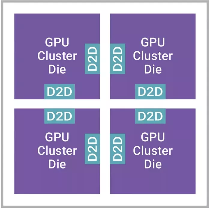
Figure 1: Die splitting use case for 100Tb switch
AI accelerators, like the Google Tensor Processor Unit, use multi-die designs by having a separate compute die and IO die for interfaces like PCIe and Ethernet. Such AI processors take advantages of multi-die designs by leveraging IO dies on a more mainstream technology process for cost savings purposes and compute dies on a more advanced technology process for performance and power purposes. Some AI accelerators use the die splitting approach, as shown in Figure 3, where high-bandwidth die-to-die interfaces are required for seamless data movement between dies.
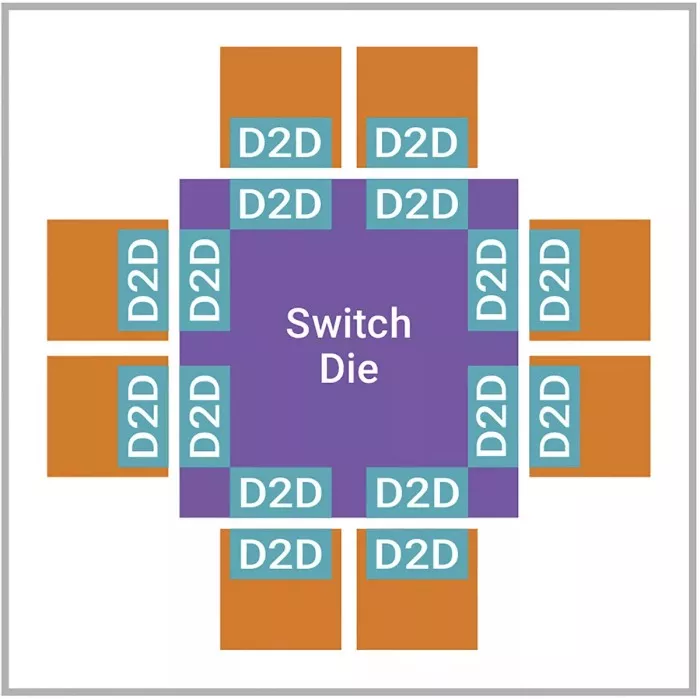
Figure 2: Die Splitting use case with an AI Accelerator
Another example is a die attachment use case where a main server die, or processor, is attached to an AI accelerator die for tasks that can be offloaded to an accelerator performing a distinct function. In this use case, the die-to-die interface is used to send the data from the server die to the accelerator die when required without having to run at high bandwidth. Such a use case uses standard packaging technology, like organic substrate, with less complexity. Many edge AI and mobile applications use these types of use cases.
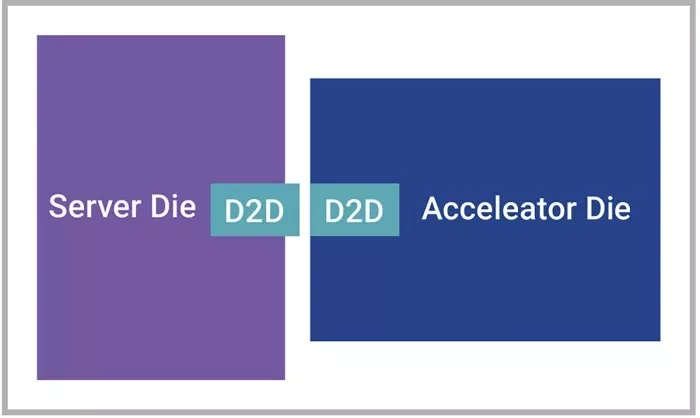
Figure 3: Die attachment use case
Delivering Maximum Bandwidth for Die-to-Die Connectivity with 40G UCIe IP
The UCIe specification has become the de facto standard for die-to-die connectivity, ensuring interoperability, low latency, and real time data movement between dies. Applications such as 100Tb switches and AI accelerators implementing the multi-die design technology leverage UCIe to enable standard and advanced packaging with maximum bandwidth efficiency. Synopsys, a contributing member of the UCIe Consortium, has built on its current silicon-proven UCIe IP to deliver a 40G UCIe IP solution that delivers 25% higher bandwidth than the UCIe specification without impacting energy efficiency or area.
The 40G UCIe PHY, compliant with the latest UCIe specification, implements various features for die-to-die link reliability and quality. The PHY offers improved testability with comprehensive design-for-test (DFT) features for known good dies and production testing. Embedded Signal Integrity Monitors (SIMs) enable mission mode monitoring of the die-to-die link. The monitors allow the continuous analysis of the die-to-die signal quality and execute corrections in mission mode for a reliable communication.
The PHY supports interface widths of up to 128B at 2GHz to consume the total PHY bandwidth. It also supports a wider 256B interface at 1GHz for systems that must operate at lower clock rates. The 40G UCIe controller supports different interface options such as streaming, CXS, AXI, and protocols like PCIe, CXL, AXI and CHI C2C to run standardized data across the die-to-die link.
While higher data rates help AI applications achieve high-bandwidth efficiency and meet data processing requirements, they impose design challenges. The channel specification must be carefully designed to avoid higher insertion loss and crosstalk to achieve best performance. At lower speeds, the transmitter (TX) equalization may not be necessary, but at higher data rates, TX equalization such as 2-tap Feed-Forward equalization (FFE) is required to achieve the required channel performance. In addition, stronger receiver (RX) equalization techniques need to be implemented such as 1 tap Decision Feedback Equalization (DFE) with Continuous Time Linear Equalization (CTLE). The die-to-die channels need to run through extensive signal integrity and power integrity simulations to verify the expected die-to-die link characteristics and performance.
Figure 4 shows an example of a lossy channel and Figure 5 shows a good channel with better design and equalization techniques.
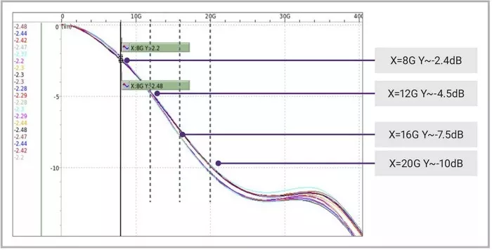
Figure 4: Example of lossy channel at 16G Nyquist frequency
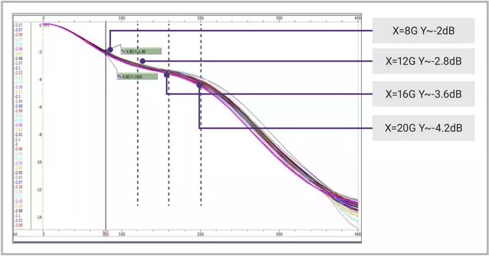
Figure 5: Example of good channel design
The 40G UCIe PHY supports the emerging advanced packaging technologies such as silicon or RDL interposer, silicon bridge and RDL fanout, and traditional organic substrate packaging technologies. The PHY delivers aggregate bandwidth efficiency of up to 12 Tbps/mm for advanced packaging technology and up to 1.8 Tbps/mm for standard packing technology, while operating up to 40Gbps/pin. While organic substrate packaging technologies are more common and cost effective, they need more routing layers to support the IP for higher speed routing. Conversely, advanced packaging technologies allow better routing density with added challenges on the package design. Understanding the complexity, Synopsys offers the 3DIC Compiler platform for Interposer design with UCIe-A IP reference design. 3DIC Compiler, a unified exploration-to-signoff platform, has tools and scripts for automated routing and custom interposer design.
The 40G UCIe IP implements a forward clock architecture to simplify the receiver architecture, reducing power and latency. It uses quad rate architecture to limit the PHY operation to 8 GHz for 32 Gbps/pin and 10 GHz for 40 Gbps/pin speeds. There are embedded low latency FIFOs to compensate for skew mismatched between forwarded and local clock and between different lanes. A common 100MHz reference clock is used as input to the PHY Phase-Locked Loop (PLL) which generates all the required high frequency clocks by the PHY and controller. This eliminates the need for the logic to provide a high frequency clock to the PHY. Figure 6 shows the 40G UCIe PHY architecture.

Figure 6: UCIe PHY Architecture
What is next for UCIe?
3D packaging is emerging as a solution for fastest multi-die designs, offering benefits in power and performance.
The UCIe specification 2.0 is standardizing the die-to-die connectivity in 3D packaging which will offer higher bandwidth and lower power compared to 2D and 2.5D technologies. The UCIe specification defines the following features for 3D packaging:
- Minimalistic PHY architecture such as simple inverter/driver
- Circuit and logic to fit within the bump area which will mean low operating frequencies and simpler circuits
- Smaller bump pitches ex. few um
- Pre-defined bump PHY bump map to simplify interoperation
Synopsys enables die-to-die connectivity in 3D packaging with the 3DIO IP solution.
In parallel to new 3D packaging, the ever-increasing demand for higher data rates is likely to be prevalent for years to come. The die-to-die interfaces will keep evolving to support higher speeds with the highest energy efficiency.
The industry’s first 40G UCIe IP solution, including controller, PHY, and verification IP, addresses the increased compute performance of the world’s fastest UCIe-based multi-die designs. The PHY’s simplified architecture eases IP integration and the comprehensive monitoring, test, and repair features enhance reliability and silicon health. Synopsys is on the forefront of the technology evolution and will continue to deploy advanced IP that supports the evolving market requirements. Visit the Synopsys 40G UCIe IP web page for more information.
Related Semiconductor IP
- UCIe D2D Adapter
- UCIe Die-to-Die Chiplet Controller
- Verification IP for UCIe
- UCIe Die-to-Die Controller IP
- UCIe Die-to-Die PHY
Related White Papers
- 40G UCIe IP Advantages for AI Applications
- Selection of FPGAs and GPUs for AI Based Applications
- Menta eFPGA IP for Edge AI
- Generative AI for Analog Integrated Circuit Design: Methodologies and Applications
Latest White Papers
- Ramping Up Open-Source RISC-V Cores: Assessing the Energy Efficiency of Superscalar, Out-of-Order Execution
- Transition Fixes in 3nm Multi-Voltage SoC Design
- CXL Topology-Aware and Expander-Driven Prefetching: Unlocking SSD Performance
- Breaking the Memory Bandwidth Boundary. GDDR7 IP Design Challenges & Solutions
- Automating NoC Design to Tackle Rising SoC Complexity