7nm networking platform delivers unprecedented performance and configurability for data center ASICs
eSilicon sets a new standard in design efficiency to enable next-generation hyperscale data centers
SAN JOSE, Calif. — June 26, 2018 — eSilicon, an independent provider of FinFET-class ASICs, market-specific IP platforms and advanced 2.5D packaging solutions, announced today the availability of a complete, highly configurable 7nm IP platform targeted for networking and data center applications.
Meeting the power, performance and density requirements of advanced networking-class ASICs is a significant challenge for system OEMs. Next-generation 12.8, 25.6 and 51.2 Tb/s switches and routers demand extreme flexibility in system architecture, I/O bandwidth and memory subsystems to achieve the required performance at a commercially acceptable power and density. eSilicon’s 7nm IP platform delivers a complete ecosystem of networking-optimized IP with high configurability designed in. All IP in the platform is “plug and play,” using the same metal stack, reliability requirements, operating ranges, control interfaces and DFT methodology. This configurability and compatibility results in better performance, higher density and faster time to market.
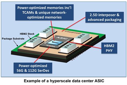
The platform includes high-performance, extremely flexible 56G and 112G SerDes, a ternary content-addressable memory (TCAM) compiler, a robust and programmable high-bandwidth memory gen2 (HBM2) PHY, multiple network-optimized memory compilers and extended-voltage general-purpose and LVDS I/Os. Along with eSilicon internally developed IP, the platform is completed with plug-and-play partner IP for functions such as PCI Express PHY, controllers, PLL and PVT monitor.
At the core of the platform is eSilicon’s SerDes technology, a new breed of performance and versatility based on a novel DSP-based architecture. Two 7nm PHYs support 56G and 112G NRZ/PAM4 operation to provide the best power efficiency tradeoffs for server, fabric and line-card applications. The architecture delivers unprecedented power efficiency for a true long-reach capability, with hole-free operation down to 1 Gb/s. The clocking architecture provides extreme flexibility to support multi-link and multi-rate operations per SerDes lane. A multitude of protocols are supported including Ethernet and Fibre Channel. The architecture allows scaling power consumption even further for shorter-reach channels.
In addition to outstanding performance and versatility, eSilicon’s SerDes technology provides a new level of usability for the ASIC design and signal integrity communities. Leveraging a decade of experience integrating complex SerDes into networking ASICs, eSilicon incorporated this unique knowledge into its SerDes family. The result is a new-to-the-market, customer-centric SerDes that is easy to integrate and easy to use.
eSilicon has delivered 12 generations of TCAM technology and is the first choice for tier-one networking customers. The current 7nm compiler supports low-power operation with partial-pipelined search, resulting in unprecedented power savings. BIST enhancements allow faster design cycles and simulation through soft programming. A patented Duo architecture and two-cycle read/write architecture reduce area and power even further for large networking ASICs.
The HBM2 PHY leverages eSilicon’s long-standing experience developing high-bandwidth, resilient and power-efficient PHYs to help address the memory bandwidth requirements of modern networking switches and routers. eSilicon’s HBM2 PHY integrates unique features to minimize switching noise and duty cycle distortion to provide a risk-free, robust solution. The PHY is a self-contained, hardened macro that offers many programmable hooks to architects. Drive strength calibration for maximum eye opening and jitter reduction as well as dedicated circuitry for training and lane repair are just two of the many features integrated to minimize time to market. eSilicon also offers a 2.5D HBM enablement package. Based on seven years of 2.5D design and integration experience, this package provides easy integration of the HBM2 PHY and associated HBM2 DRAM stacks.
Rounding out the platform is an array of unique, network-optimized, high-speed and ultra-high-density memory compilers, register files and latch-based compilers optimized for extreme density and performance. Embedded BIST is available as an option to provide optimal DFT coverage, save area on large memories and reduce designers’ efforts in synthesis, timing closure and routing congestion. The platform also includes networking-optimized extended-voltage and LVDS I/Os.
“Networking applications at 25Tb/s and above demand a configurable architecture to quickly balance power, performance and density requirements,” said Hugh Durdan, vice president of strategy and products at eSilicon. “Our 7nm platform now offers a complete and robust solution to these design challenges thanks to its extreme configurability, making hyperscale data center technology within reach for more system OEMs.”
Several tier-one system OEMs are actively evaluating eSilicon’s new 7nm platform for their next-generation products.
To learn more, contact your eSilicon sales representative or visit eSilicon’s 7nm IP networking platform web page. This latest platform offering from eSilicon adds to the recently announced 7nm neuASICä platform for machine learning ASIC design.

About eSilicon
eSilicon is an independent provider of complex FinFET-class ASICs, market-specific IP platforms and advanced 2.5D packaging solutions. Our ASIC+IP synergies include complete 2.5D/HBM2 and TCAM platforms for FinFET technology at 16/14/7nm as well as SerDes, specialized memory compilers and I/O libraries. Supported by patented knowledge base and optimization technology, eSilicon delivers a transparent, collaborative, flexible customer experience to serve the high-bandwidth networking, high-performance computing, artificial intelligence (AI) and 5G infrastructure markets. www.esilicon.com
Related Semiconductor IP
- UCIe D2D Adapter & PHY Integrated IP
- Low Dropout (LDO) Regulator
- 16-Bit xSPI PSRAM PHY
- ASIL B Compliant MIPI CSI-2 CSE2 Security Module
- SHA-256 Secure Hash Algorithm IP Core
Related News
- Broadcom Announces Industry's First Silicon-Proven 7nm IP for ASICs in Deep Learning and Networking Applications
- eSilicon announces 7nm FinFET ASIC design win
- The Linley Group Microprocessor Report Details eSilicon 7nm IP
- eSilicon Announces Silicon Validation of 7nm 56G SerDes
Latest News
- Perceptia Devices and Dolphin Semiconductor Partner to Deliver Best-in-Class IP Portfolio Covering Power Management, Clocking, High-Quality Audio and In-Situ Monitoring
- TSMC Chases Soaring AI Demand
- EU DARE Project Is Scrambling to Replace Codasip
- Sofics and Alcyon Photonics Partner to Support Next-Generation Photonic Systems
- QuickLogic Appoints Quantum Leap Solutions as Authorized Sales Representative