Attopsemi Technology Presented "I-fuse: Dream OTP Finally Comes True" and won the best Innovative IP award on IP SoC 2019 China
Hsinchu, Taiwan –September 18, 2019 – Attopsemi Technology attended D&R IP SoC Day on September 12, 2019 in Shanghai, China and provided a talk “I-fuse™: Dream OTP Finally Comes True” and won the best Innovative IP award.
In a well-received speech during the Technical Session, Shine Chung, Chairman of Attopsemi, presented the topic “I-fuse™: Dream OTP Finally Comes True” In the OTP(One-Time Programmable) IP market. Defying the conventional wisdom of breaking a fuse to maintain a permanent programmed state forever, Attopsemi’s I-fuse™ is actually a “non-breaking” fuse. “I don’t mind to break a fuse, but I do care about breaking a fuse by explosion”, said Shine Chung, Chairman of Attopsemi. “The I-V curve of programming a fuse after the break point actually show the behavior is more like an explosion. The SEM photos do confirm this. After explosion, debris can be created and micro-bridged again and become shorts to cause severe reliability problems.” “On the other hand, the I-V curves showed very smooth and repeatable curves, if the programming is below the break point and above the electromigration threshold,” further explained by Shine Chung.
With a twist of mindset, all the good attributes of an OTP show up. Program current/voltage can be lower. Cell/IP size can be smaller. High temperature, high reliability, and high data security can be achieved because of less damage to the fuse body. The program voltage can be inlined with I/O voltages, or can even be core voltages with some area penalties. In fact, I-fuse™ is more like a logic device that can be read at sub-VDD and consume only 1/100 of read energy, comparing with the conventional sensing, for energy harvest. I-fuse™ can also be built as bit cell in any standard cell libraries so that low-bit-count I-fuse™ OTP can be built by standard logic design flow.
Comparing with the other OTP technologies on 22nm and beyond, I-fuse™ can be programmed at 1.0V, while the other anti-fuses need 4-5V to program. I-fuse™ can be programmed at 1.0mA, while the eFuse needs up to 100mA to program.
A dream OTP, I-fuse™, finally comes true.
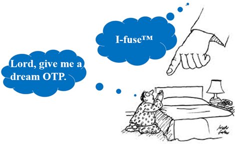
Dream OTP Finally Comes True.
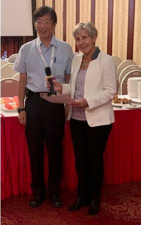
Shine Chung, Chairman of Attopsemi (left) Presented “I-fuse™: Dream OTP Finally Comes True” and won the best IP prize in IP SoC 2019 China.
https://www.design-reuse-embedded.com/ipsocdays/ipsocdays2019/china2019/files/bio/BestPrize.jsp
About Attopsemi Technology
Founded in 2010, Attopsemi Technology is dedicated to developing and licensing fuse-based One-Time Programmable (OTP) IP to all CMOS process technologies from 0.7um to 7nm and beyond in various silicided polysilicon, HKMG, FDSOI and FinFET technologies. Attopsemi provides the best possible OTP solutions for all merits in small size, low voltage/current programming/read, high quality, high reliability, low power, high speed, wide temperature and high data security. Attopsemi's proprietary I-fuse™ OTP technologies have been proven in numerous CMOS technologies and in several silicon foundries.
Related Semiconductor IP
- OTP
- Secure Storage Solution for OTP IP
- GF 22FDX 5.5V OTP Auto-Grade1 IO Staggered
- GF 22FDX 5.5V OTP Auto-Grade1 IO Inline
- NVM OTP XBC TSMC N7 1.8V
Related News
- Innosilicon to Showcase High-Speed Interface IP and Advanced SoC Solutions at the 2025 TSMC OIP Ecosystem Forum
- Silicon Creations Receives 9th Consecutive TSMC OIP Partner of the Year Award for Mixed Signal IP
- Alphawave Semi Achieves 2025 TSMC OIP Partner of the Year Award for High-Speed SerDes IP
- EagleChip Selects CAST TSN IP Core to Enhance Advanced Intelligent Control SoC
Latest News
- Sofics and Alcyon Photonics Partner to Support Next-Generation Photonic Systems
- QuickLogic Appoints Quantum Leap Solutions as Authorized Sales Representative
- Cadence and NVIDIA Expand Partnership to Reinvent Engineering for the Age of AI and Accelerated Computing
- Cadence and Google Collaborate to Scale AI-Driven Chip Design with ChipStack AI Super Agent on Google Cloud
- Analog Bits Demonstrates Real-Time On-Chip Power Sensing and Delivery on TSMC N2P Process at TSMC 2026 Technology Symposiums