Sofics IP
Filter
Compare
6
IP
from
1
vendors
(1
-
6)
-
1.2V Thin Oxide GPIO on TSMC 28nm RF HPC+
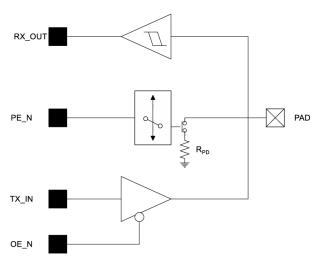
- The 1.2V Thin Gate GPIO is an IP macro for on-chip integration. It is a 1.2V general purpose I/O that does not rely on thick-gate devices. Only thin-gate, 0.9V capable core MOS devices are used in the design.
- Supported features include core isolation, programmable slew rate compensation, programmable drive strength, input/output enable, pull select and pull enable. Extra features such as programmable hysteresis can be supported upon request.
-
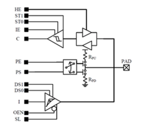
1.8V Capable GPIO on Samsung Foundry 4nm FinFET
- The 1.8V capable GPIO is an IP macro for on-chip integration. It is a 1.8V general purpose I/O built with a stack of 1.2V MOS FINFET devices. It is controlled by 0.75V (core) signals.
- Supported features include core isolation, output enable and pull enable. Extra features such as input enable/disable, programmable drive strength and pull select, can be supported upon request.
-
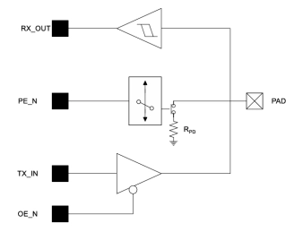
3.3V Capable GPIO on TSMC 28nm RF HPC+
- The 3.3V capable GPIO is an IP macro for on-chip integration. It is a 3.3V general purpose I/O built with a stack of 1.8V thick oxide MOS devices. It is controlled by 0.9V (core) signals.
- Supported features include core isolation, output enable and pull enable. Extra features such as input enable/disable, programmable drive strength and pull select, can be supported upon request.