PLL DLL IP
Filter
Compare
22
IP
from
11
vendors
(1
-
10)
-
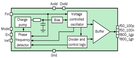
Ring oscillator-based analog PLL
- Our ring oscillator-based analog PLL provides good phase noise performance with extremely low energy consumption and small area compared to the state-of-the-art products.
- The programmable divider allows to shift the output frequency with a large locking range.
-
800/1000 MHz DLL-based frequency multiplier
- TSMC 90 nm CMOS
- Low jitter
- Precisely aligns the clock distribution output with a reference clock
- Low current consumption
-
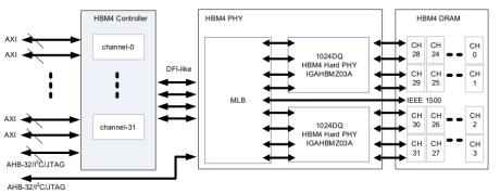
TSMC CLN3FFP HBM4 PHY
- IGAHBMZ03A is a High Bandwidth Memory 4 Physical Layer (HBM4 PHY) that is compliant with JEDEC HBM4 DRAM Specification JESD270-4.
- Fabricated in the TSMC 3 nm Advanced process node (N3P), it supports the data rate up to 12 Gbps per data pin in the DDR PHY Interface (DFI)-like 1:4 clock frequency ratio (HBM4 controller clock: WDQS = 1:4).
-
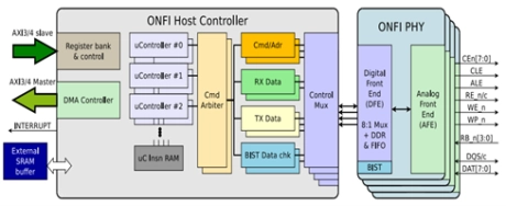
ONFI 3.2 NAND Flash Controller IP Compliant to JEDEC
- Compliant to ONFI 3.2 Specification
- Supports SDR, NV-DDR and NV-DDR2
- Included synthesizable PLL/DLL
- ONFI 3.2 compatible 1.8v NV-DDR2 I/O pads supporting up to 533MT/s is available

-
ONFI 5.0 NAND Fash PHY IP Compliant to JEDEC
- The ONFI 5.0 PHY IP is designed to connect seamlessly with their ONFI 5.0 Host Controller IP.
- The ONFI 5.0 PHY has complete SDR, NV-DDR, NV-DDR2, NV-DDR3 and NV-LPDDR4 TX/RX functionality and supports all the speeds defined in the ONFI specification while remaining backwards compatible with the prior versions of the ONFI specifications.
-
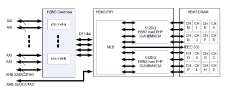
TSMC CLN7FF HBM3 PHY
- IGAHBMX03A is a HBM3 (High Bandwidth Memory) PHY IP compliant to the JEDEC HBM3 DRAM Specification Rev 0.95.
- Built on TSMC 7nm process node, it supports data rate up to 7200 Mbps per data pin with DFI 1:4 clock frequency ratio (controller clock : WCK = 1:4).
-
LPDDR 4/4X PHY, TSMC 12E, N/S orientation
- Multi-interface support: LPDDR4 up to 4267Mbps, LPDDR4X up to 4267Mpbs
- Supports LPDDR4X 0.6V VDDQ
- Optimized for high performance and integration flexibility. The harden IP included 8-bit data blocks, 6-bit C/A blocks, clock blocks, PLL and DLL. IP pin-out can be configured to optimize for LPDDR4/4X.
- High resolution read/write timing control
-
DDR4/LPDDR4/LPDDR4X PHY
- Multi-interface support. LPDDR4 up to 3200Mbps and DDR4/LPDDR4X up to 4267Mpbs.
- Support LPDDR4X 0.6V VDDQ.
-
TSMC CLN7FF HBM2E PHY IP
- High Bandwidth Memory (HBM2E) DRAM PHY
- Supports HBM 3.2Gbps
- Supports DFI 1:2
- Supports only BL4
-
TSMC CLN5FF HBM PHY IP
- High Bandwidth Memory (HBM) DRAM PHY
- Supports HBM 3.6Gbps
- Supports DFI 1:2
- Supports only BL4