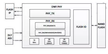
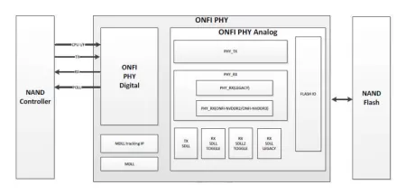
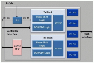
ONFI PHY IP
Filter
Compare
21
IP
from
11
vendors
(1
-
10)
-
ONFI PHY 4.8GT/s for ONFI v6 & JESD230G
- Multi-interface support: ONFI6.0 up to 4800Mbps
- Multi-data-interface support: CTT (NVDDR3), LTT (NVLPDDR4) and PI-LTT
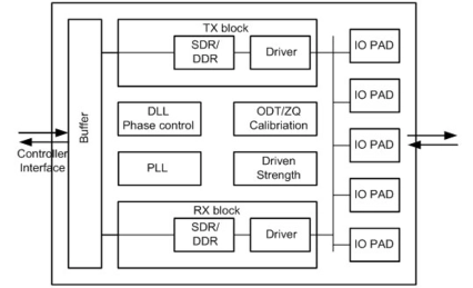
- Optimized for high performance and integration flexibility. The harden IP included 8-bit data blocks, up to 8 CE/channel, clock blocks, PLL, and DLL.
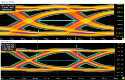
- High-resolution read/write delay adjust
-
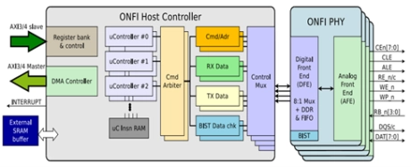
ONFI PHY & Controller
- The ONFI IP provides Turnkey solutions for IC requiring access to ONFI-compatible NAND Flash devices
- Optimized for low power and high-speed applications, it features robust timing and a compact silicon area
- It supports all ONFI NAND Flash components available on the market
-
ONFI NAND PHY
- ONFI 1/2/3/4/5 compliant
- SLC/MLC/TLC support
- SDR (Asynchronous) mode 0 to 5
- NV-DDR (Source Synchronous) mode 0 to 5
- NV-DDR2 mode 0 to 10
-
ONFI 5.1 PHY IP
- Compliant with ONFI 5.1 specification
- Supports NV-DDR3/NV-LPDDR4, with a maximum rate up to 3600MT/s
- Supports matched or unmatched DQS
- Supports WDCA/Per-Pin VREFQ Training for NAND devices
-
ONFI 5.0 PHY IP
- Compliant with ONFI 5.0 specification
- Supports NV-DDR2 mode
- Supports NV-DDR3, NV-LPDDR4, with a maximum rate of 2400MT/s
- Supports PHY Independent TX/RX Training mode
-
ONFi PHY 4.0 (FPHY+MDLL+SDLL Regulator) (Silicon Proven in TSMC 28HPC+)
- Support ONFi 4.0 IO Electrical Specification
- Support Legacy up to 50MHz
- Support NV-DDR2 with operating frequency up to 533Mbps
- Support NV-DDR3 with operating frequency up to 800Mbps
-
ONFI 4.1 PHY IP (Silicon Proven in TSMC 12FFC)
- Support ONFi 4.1 IO Electrical Specification
- Support Legacy up to 50MHz
- Support NV-DDR2 up to 533Mbps
- Support NV-DDR3 up to 1200Mbps
-
ONFI 3.2 NAND Flash PHY IP Compliant to JEDEC
- Compliant to ONFI revision 3.2 standard
- Silicon proven PLL to support all frequencies from 10MHz to 266MHz, and DLL to improve data sampling accuracy dynamically
- Include ONFI 3.2 I/O pads compatible to 1.8v NV-DDR2 533 MT/s and 3v NV-DDR 200 MT/s
- Supports NV-DDR2 mode of operation supporting up to 266MHz
-
ONFI 5.0 NAND Fash PHY IP Compliant to JEDEC
- The ONFI 5.0 PHY IP is designed to connect seamlessly with their ONFI 5.0 Host Controller IP.
- The ONFI 5.0 PHY has complete SDR, NV-DDR, NV-DDR2, NV-DDR3 and NV-LPDDR4 TX/RX functionality and supports all the speeds defined in the ONFI specification while remaining backwards compatible with the prior versions of the ONFI specifications.