GDDR7 IP
Filter
Compare
9
IP
from
5
vendors
(1
-
9)
-
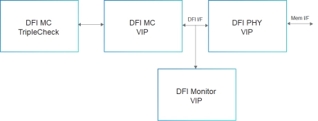
GDDR7 Synthesizable Transactor
- Supports GDDR7 memory devices from all leading vendors.
- Supports 100% of GDDR7 protocol draft JEDEC specification.
- Supports all the GDDR7 commands as per the specs.
- Supports 4 separate independent channels with point-to-point interface for data, address and command.
-
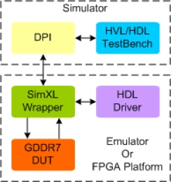
GDDR7 Memory Model
- Supports GDDR7 memory devices from all leading vendors.
- Supports 100% of GDDR7 protocol draft JEDEC specification.
- Supports all the GDDR7 commands as per the specs.
- Supports 4 separate independent channels with point-to-point interface for data, address and command.
-
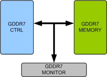
GDDR7 DFI Verification IP
- Compliant with DFI version 4.0 or 5.0 Specifications.
- Supports GDDR7 devices compliant with GDDR7 SGRAM draft specification.
- Supports all Interface Groups.
- Supports Write Transactions with Data mask.
-
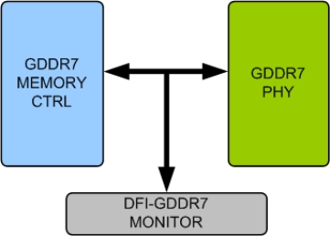
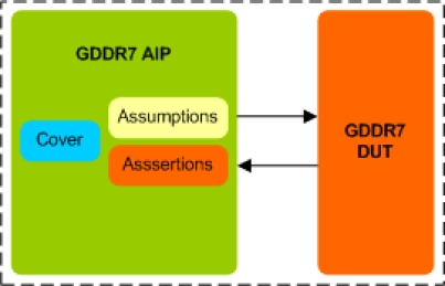
GDDR7 Assertion IP
- Specification Compliance
- Supports GDDR7 memory devices from all leading vendors.
- Supports 100% of GDDR7 protocol draft JEDEC specification.
- Supports all the GDDR7 commands as per the specs.
-
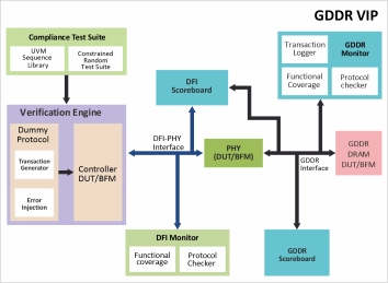
GDDR 7 Verification IP
- Compliant to JEDEC JESD239A GDDR7 Specification.
- Supports connection to any GDDR7 Memory Controller IP communicating with a JEDEC compliant GDDR7 Memory Model.
- Available in all memory sizes from upto 64Gb.
- Command Supported
- Write: Write, Write Auto-Precharge
- Read: Read, Read Auto-Precharges
- Mode Register Set, Activate, Load FIFO
- Precharge: PREab, PREb
- Refresh: REFab, REFpb
- Refresh Management: RFMab, RFMpb
- Power Down Entry (PDE), Power Down Exit (PDX)
- Self-Refresh Entry (SRE), Self-Refresh Exit (SRX)
- Sleep Entry, Self-Refresh Sleep Entry
- Training Commands
-
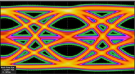
GDDR7 PHY
- Highest performance at 36Gbp/s
- Fully hardened timing-closed PHY
- Available in multiple advanced-process nodes
- PAM3 signaling or NRZ
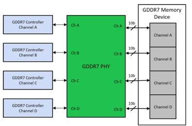
- 4 independent channels
- PHY independent mode
- Microcontroller or state machine training
- Low-power clock gating
-
GDDR7 PHY & Controller
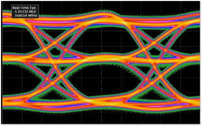
- The GDDR7 PHY is fully compliant with the JEDEC GDDR7 standard, supporting data rates of up to 32 Gbps in PAM3 mode
- In PAM3 mode, each byte consists of ten DQ signals and one DQE signal, while the GDDR7 also supports NRZ I/O signaling for low-power operation
- With a maximum speed of 32 Gbps per pin, The GDDR7 PHY delivers a peak bandwidth of up to 128 GB/s per memory device
-
GDDR7 Memory Controller
- Supports up to 40 Gbps per pin operation
- 2.5 GHz CK4 clock
- 1.25 GHz controller clock
- Internal data path 32x memory width (i.e. 256 bits for 8-bit memory)
- Optimized for high efficiency and low latency across a wide range of traffic scenarios (random/sequential, short/long bursts, etc.)
- Optimized command sequence for highest bus utilization including per-bank refresh scheduling: single queue structure handles look-ahead activates/ precharges and read/write ordering for minimal latency
-
Simulation VIP for DFI
- DFI MC
- Command Interface
- Drives Command on different phases based on memory protocol requirement
- DDR4-5, LPDDR4-5, HBM2E-3 and GDDR6-7
