DDR2 Controller IP
Welcome to the ultimate DDR2 Controller IP hub! Explore our vast directory of DDR2 Controller IP
All offers in
DDR2 Controller IP
Filter
Compare
33
DDR2 Controller IP
from
11
vendors
(1
-
10)
-
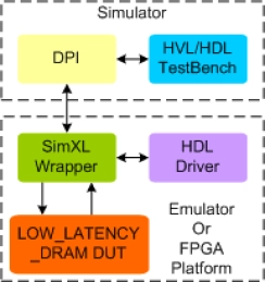
Low Latency DRAM Synthesizable Transactor
- Supports 100% of Low Latency DRAM protocol standard Low Latency DRAM specifications
- Supports 8 internal banks
- Supports all mode registers programming
- Supports programmable read latency and row cycle time
-
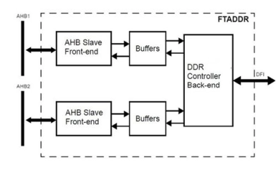
Fault Tolerant DDR2/DDR3/DDR4 Memory controller
- FTADDR is a memory controller for DDR2,DDR3 and DDR4 SDRAM memory devices.
- It uses a strong error correction code to achieve exceptional fault tolerance
-
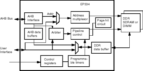
AMBA AHB Bus to DDR SDRAM Controller
- External pin reduction by transferring 2 bits of data per pin.
- Supports multiple external SDRAM banks.
- Automatic refresh generation with programmable refresh intervals.
- Self-refresh mode to reduce system power consumption.
- Standard delay cells or user provided DLL for DQ and DQS alignment.
-
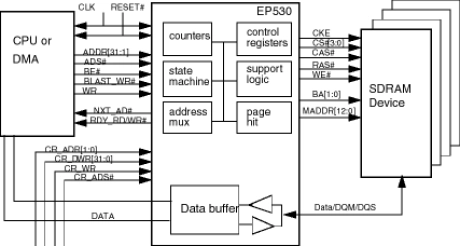
DDR SDRAM Controller
- Supports industry standard Double Data Rate (DDR) SDRAM.
- Designed for ASIC and FPGA implementations in various system environments.
- Programmable memory size and data width.
- Supports industrial standard 64Mbit, 128Mbit and 256Mbit DDR SDRAMs.
-
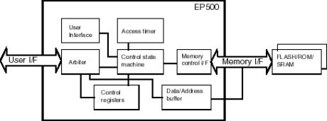
Flash/ROM/SRAM Controller
- Supports industry standard Asynchronous SRAM, NOR Flash, ROM and similar memory devices.
- Two request ports to allow two requesters to share access to the FLASH/ROM/SRAM devices.
- 8 Chip select signals to access up to 8 memory banks.
- Independent programmable timing parameters for each chip select.
-
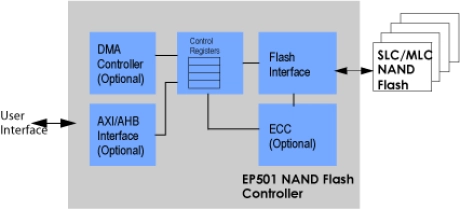
NAND Flash Controller
- Supports single-level and multi-level cells (SLC and MLC) NAND Flash devices.
- Supports 1, 4 and 8 bit ECC correction per 512byte.
- Uses Hamming code for SLC and BCH code for multi-bit correction in MLC.
- Programmable support for large block and small block NAND Flash devices with 512, 2k and 4k byte page sizes.
-
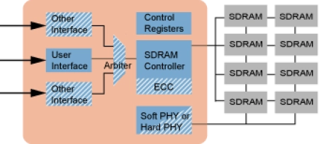
DDR2 SDRAM Controller
- Supports industrial standard Double Data Rate (DDR) and Double Date Rate2 (DDR2) SDRAM from 64Mbit to 2Gbit device sizes.
- Page hit detection to support multiple column accesses within the same row.
- Pipeline access enables continuous data bursting and hidden active commands, even in the case of page misses.
- Issue precharge, active and read/write commands to multiple banks at the same time.
-
High-Performance Memory Controller II SDRAM Intel® FPGA IP Core
- The High-Performance Memory Controller II SDRAM Intel FPGA IP core handles the complex aspects of using DDR, DDR2, and DDR3 SDRAM at speeds up to 933 MHz
- The intellectual property (IP) core initializes the memory devices, manages SDRAM banks, translates read-and-write requests from the local interface into all the necessary SDRAM command signals, and performs command and data reordering.

-
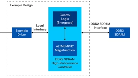
DDR and DDR2 SDRAM Controller with ALTMEMPHY Intel® FPGA IP
- The DDR and DDR2 SDRAM Controller with ALTMEMPHY Intel FPGA Intellectual Property (IP) provides simplified interfaces to industry-standard DDR SDRAM and DDR2 SDRAM
- The DDR and DDR2 SDRAM Controller with ALTMEMPHY Intel FPGA IP core work in conjunction with the ALTMEMPHY physical interface IP function
- The controllers offer a half-rate interface and a full-rate interface to the customer application logic
- For exact device support, please refer to the user guide.
-
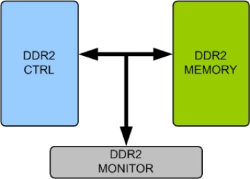
DDR2 Monitor Verification IP
- Supports DDR2 memory devices from all leading vendors
- Quickly validates the implementation of the DDR2 standard
- Constantly monitors DDR2 behavior during simulation
- Checks for following