DDR2 IP
Welcome to the ultimate DDR2 IP hub! Explore our vast directory of DDR2 IP
All offers in
DDR2 IP
Filter
Compare
35
DDR2 IP
from
12
vendors
(1
-
10)
-
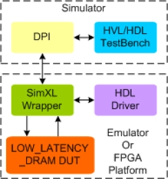
Low Latency DRAM Synthesizable Transactor
- Supports 100% of Low Latency DRAM protocol standard Low Latency DRAM specifications
- Supports 8 internal banks
- Supports all mode registers programming
- Supports programmable read latency and row cycle time
-
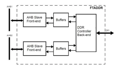
Fault Tolerant DDR2/DDR3/DDR4 Memory controller
- FTADDR is a memory controller for DDR2,DDR3 and DDR4 SDRAM memory devices.
- It uses a strong error correction code to achieve exceptional fault tolerance
-
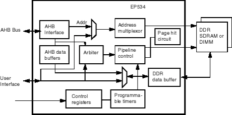
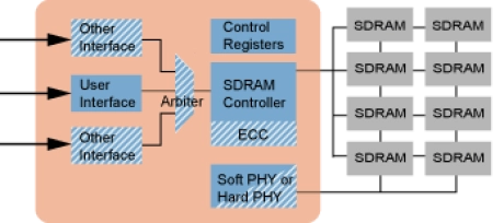
AMBA AHB Bus to DDR SDRAM Controller
- External pin reduction by transferring 2 bits of data per pin.
- Supports multiple external SDRAM banks.
- Automatic refresh generation with programmable refresh intervals.
- Self-refresh mode to reduce system power consumption.
- Standard delay cells or user provided DLL for DQ and DQS alignment.
-
DDR SDRAM Controller
- Supports industry standard Double Data Rate (DDR) SDRAM.
- Designed for ASIC and FPGA implementations in various system environments.
- Programmable memory size and data width.
- Supports industrial standard 64Mbit, 128Mbit and 256Mbit DDR SDRAMs.
-
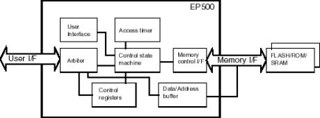
Flash/ROM/SRAM Controller
- Supports industry standard Asynchronous SRAM, NOR Flash, ROM and similar memory devices.
- Two request ports to allow two requesters to share access to the FLASH/ROM/SRAM devices.
- 8 Chip select signals to access up to 8 memory banks.
- Independent programmable timing parameters for each chip select.
-
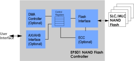
NAND Flash Controller
- Supports single-level and multi-level cells (SLC and MLC) NAND Flash devices.
- Supports 1, 4 and 8 bit ECC correction per 512byte.
- Uses Hamming code for SLC and BCH code for multi-bit correction in MLC.
- Programmable support for large block and small block NAND Flash devices with 512, 2k and 4k byte page sizes.
-
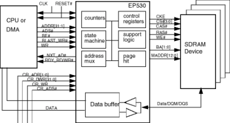
DDR2 SDRAM Controller
- Supports industrial standard Double Data Rate (DDR) and Double Date Rate2 (DDR2) SDRAM from 64Mbit to 2Gbit device sizes.
- Page hit detection to support multiple column accesses within the same row.
- Pipeline access enables continuous data bursting and hidden active commands, even in the case of page misses.
- Issue precharge, active and read/write commands to multiple banks at the same time.
-
High-Performance Memory Controller II SDRAM Intel® FPGA IP Core
- The High-Performance Memory Controller II SDRAM Intel FPGA IP core handles the complex aspects of using DDR, DDR2, and DDR3 SDRAM at speeds up to 933 MHz
- The intellectual property (IP) core initializes the memory devices, manages SDRAM banks, translates read-and-write requests from the local interface into all the necessary SDRAM command signals, and performs command and data reordering.

-
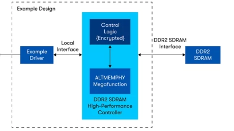
DDR and DDR2 SDRAM Controller with ALTMEMPHY Intel® FPGA IP
- The DDR and DDR2 SDRAM Controller with ALTMEMPHY Intel FPGA Intellectual Property (IP) provides simplified interfaces to industry-standard DDR SDRAM and DDR2 SDRAM
- The DDR and DDR2 SDRAM Controller with ALTMEMPHY Intel FPGA IP core work in conjunction with the ALTMEMPHY physical interface IP function
- The controllers offer a half-rate interface and a full-rate interface to the customer application logic
- For exact device support, please refer to the user guide.
-
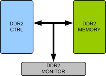
DDR2 Monitor Verification IP
- Supports DDR2 memory devices from all leading vendors
- Quickly validates the implementation of the DDR2 standard
- Constantly monitors DDR2 behavior during simulation
- Checks for following