I/O Library IP for UMC
Welcome to the ultimate
I/O Library IP
for
UMC
hub! Explore our vast directory of
I/O Library IP
for
UMC
All offers in
I/O Library IP
for
UMC
Filter
Compare
421
I/O Library IP
for
UMC
from
10
vendors
(1
-
10)
-
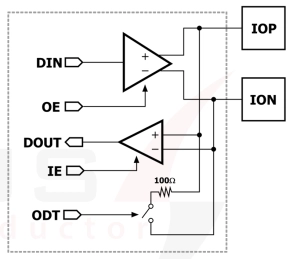
1.2V SLVS Transceiver in UMC 110nm
- This library delivers a compact and reliable 1.2V SLVS transceiver solution in UMC 110nm, optimized for high-speed, low-power applications.
- Featuring robust supply and ground noise rejection, 2kV HBM ESD protection, and integrated on die termination, this library provides both transmit and receive paths compliant with JESD8-13 SLVS standards at up to 200 Mbps.
-
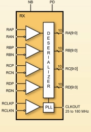
LVDS Deserializer IP
- The MXL-DS-LVDS is a high performance 4-channel LVDS Deserializer implemented using digital CMOS technology.
- Both the serial and parallel data are organized into four channels. The parallel data can be 7 or 10 bits wide per channel. The input clock is 25MHz to 165MHz. The De-serializer is highly integrated and requires no external components.
-
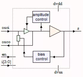
5MHz-35MHz Low Power Crystal Oscillator - TSMC 0.18µ
- 4MHz-35MHz Frequency range.
- No external bias or limit resistors required.
- Current optimization for best power at frequency.
- Amplitude control loop.
- The OSCI pad input can be used as a CMOS input for test.
- Uses single 1.8V supply.
- Enable/power down provision.
-
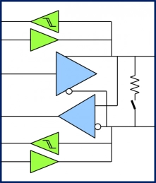
LVDS interfaces
- Wide operating range
- High data rates
- Very flexible programmability
- Excellent signal integrity
- TIA/EIA644A LVDS and sub-LVDS compatibility
- Receiver also compatible with LVPECL
-
I/O Library
- Dolphin Technology offers an extensive array of Interface IP, all of whichhasbeen optimized for ultra high performance across all processes supported.
- Our I/O portfolio includes: Standard I/O (General Purpose I/O or GPIO), Specialty I/O (bus-specific I/O), NAND Flash I/O and DDRx & LPDDRx I/O.
-
Camera 6/7-mode Combo Receiver - 1G/1.5Gbps
- The CL12684KM4-8-12-16R3AM6-7ZIP is an ideal means to link Camera Modules or CMOS Image Sensor (CIS) to Host System.
- The CL12684KM4-8-12-16R3AM6-7ZIP is designed to support data rate in excess of maximum 1Gbps utilizing sub-LVDS / mini-LVDS / LVDS / HiSPi(SLVS-400, HiVCM) / MIPI-DPHY / CMOS-1.8V / CMOS-3.3V interface specification.
-
LCD Host LVDS Interface, Dual Pixel 20-112Mhz (SVGA/QXGA)
- 1P6M layout structure based on 0.18um 1P6M 1.8V generic logic process.
- 3.3V/1.8V ±10% supply voltage, -40/+125°C
- Complies with OpenLDI specification for digital display interfaces and LVDS IEEE Standard 1596.3-1996+ ANSI/TIA/EIA-644-A Specifications.
- Up to 5.38Gbps bandwidth
-
7 way DDR combo
- Full DDR4 capability
- Full DDR3 / DDR3L / DDR3U capability
- Full LPDDR4 capability
- Full LPDDR3 capability
-
General-Purpose I/O (GPIO) - 1.5V-1.8V
- ? Multi-Voltage (1.2V, 1.5V, 1.8V)
- ? LVCMOS / LVTTL input with selectable hysteresis
- ? Programmable drive strength (rated 2mA to 12mA)
- ? Selectable output slew rate