Chip Design Industry Reaches an AI Inflection Point
The chip design landscape has hit a transformative milestone, one that signals a turning point in how semiconductors are conceived, developed, and brought to market. AI-powered tools, which first emerged as niche solutions in the realm of Electronic Design Automation (EDA), have now become indispensable in advanced chip design. In a recent article, Bob O'Donnell, Technalysis, describes that what was once an experimental frontier has now crossed a critical threshold, where over 50% of advanced silicon designs (process nodes of 28nm and below) are being realized with AI assistance. The era of AI-driven chip design is no longer a distant horizon; it’s become the new status quo.
Understanding the AI Inflection Point in Chip Design
An inflection point represents a seismic shift in a trajectory, and for the semiconductor world, that moment arrived in Q1 2025. Cadence has reported over 1,000 customers have successfully taped out on <=28nm using its AI-driven chip implementation platform, Cadence Cerebrus. When consolidated with other vendors disclosed tapeout data, and analyzed as estimated quarterly increments, these achievements signal a universal adoption shift, where AI-led methods are now anchoring semiconductor innovation at advanced technology nodes.
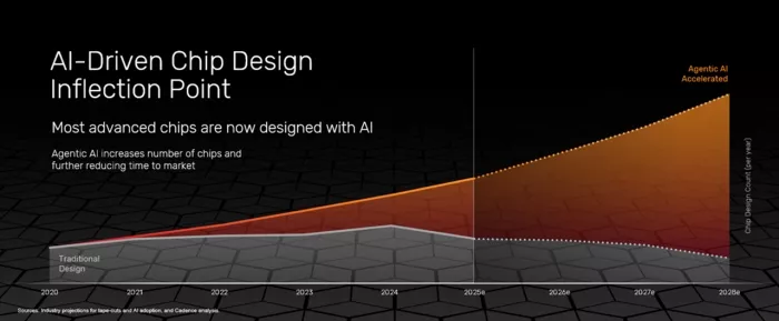
Figure 1: The Inflection Point of AI-driven Digital Chip Design in Q1 2025
But why is this inflection point significant? Historically, chip design has been a domain dominated by intricate calculations, relentless iteration, and the critical path in time-to-market. The increasing complexity of chip architectures, especially with the rise of AI in data centers and at the edge, made manual and traditional approaches unsustainable. AI-driven chip design has become a necessity, not to assist incrementally but to fundamentally redefine the workflows involved.
The Impact of AI on Chip Design
AI’s revolution in chip design is multifaceted. Companies leveraging AI tools are seeing remarkable boosts in chip quality, performance, and time-to-market. For example, during CadenceLIVE 2023, a leading provider of smart, connected, and secure embedded control semiconductors reported a tenfold productivity improvement, reducing an advanced 6nm networking chip design tapeout timeline from six weeks to just two weeks. Similarly, their CPU design process at the same technology node dropped from five weeks to only twelve days.
These efficiency breakthroughs not only save time but also translate to higher ROI. Reducing a project’s timeline by weeks improves a company's competitiveness and decision-making agility. Productivity jumps of 5-10x are typical, allowing organizations to complete more projects, explore more design permutations, and roll out optimized solutions. Ultimately, this equates to faster innovation cycles, better-performing semiconductors, and a quicker delivery of critical AI applications like generative AI, high-performance computing, and data center infrastructure.
Beyond productivity, AI-powered design tools impact improving first-time silicon success rates. This is vital, as mistakes can not only delay a project but derail it entirely. AI algorithms can identify inefficiencies and design risks early on, helping mitigate issues that would otherwise surface late in the fabrication stage.
Implications for the Semiconductor Industry
For the semiconductor industry, this AI-driven inflection point heralds an unprecedented era of possibilities. Major hyperscalers, along with device giants, are now vying for dominance in custom chip development. One critical bottleneck has been the world’s limited pool of elite chip designers. Here, AI serves as a democratizer, empowering smaller teams, less experienced designers, and even organizations outside traditional semiconductor spaces to develop their own chips with cutting-edge functionalities.
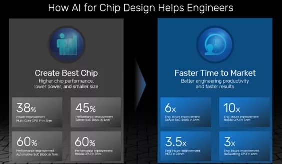
Figure 2: AI-Driven Chip Design Impact on Products and Schedules
The shift also enables the industry to address an age-old dilemma: creating highly customized designs at scale. Historically, bespoke silicon was frequently deemed too expensive or time-consuming. Now, AI-supported workflows make varied, application-specific designs feasible without overwhelming cost or resource demands.
Semiconductor pioneers and industry leaders alike are increasingly adopting AI-driven methodologies to pioneer next-generation chips designed to power AI applications themselves. This virtuous cycle of AI designing AI amplifiers is driving exponential growth in the sector, fueling predictions that the semiconductor market will expand to $1T by 2029 (source: IBS Monthly Report, May 2024), with generative AI and high-performance computing as primary accelerators.
ROI of AI in Chip Design
AI's value in chip design is becoming essential. The combination of reduced time-to-market and enhanced chip performance is now a competitive differentiator. Whether it’s saving two months on an advanced-node project or achieving a substantial performance boost on specific chip blocks, the financial and strategic value derived from these tools underscores their necessity.
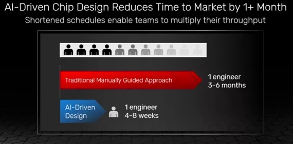
Figure 3: AI-Driven Chip Design Time-to-Market Impact
Unlike other AI applications that are searching for a path to financial impact, chip design is a tangible success story. For example, shifting a design timeline from eight months to six is not only an economic benefit, but can tip a product trend in your favor. The ability to deliver high-performing processors faster and at a lower risk is the kind of concrete benefit leading to wide spread adoption.
What’s Next for AI in Chip Design?
The future of AI in chip design is as promising as it is profound. AI methodologies are expanding beyond chip optimization to system-level design and analysis. Agentic AI, for instance, promises to automate workflows further, unlocking new efficiencies and enabling engineers to focus on higher-value tasks.
Meanwhile, technologies like the agentic AI are being designed to support groundbreaking initiatives in infrastructure AI, physical AI, and sciences AI. These advances will redefine fields ranging from drug discovery to next-generation reality systems. Just as importantly, the evolution of AI-powered platforms will make it possible to design chips for entirely new applications, particularly in energy-constrained environments.
Looking ahead, we can expect the widespread adoption of AI-driven systems design to follow the current momentum in chip design. From self-powered IoT devices to AI-driven robotics, the proliferation of custom chips will fuel innovation across countless industries.
Final Thoughts
The semiconductor industry is entering a bold new chapter, one where AI is no longer an auxiliary tool but a central pillar of innovation. The AI inflection point in chip design isn’t just about speeding up processes or reducing costs; it’s about redefining what’s possible. As we move forward, the lines between AI, chip design, and system-level engineering will blur, creating a virtuous cycle of technological advancement that will propel the next wave of digital transformation.
Related Semiconductor IP
- SHA-256 Secure Hash Algorithm IP Core
- EdDSA Curve25519 signature generation engine
- DeWarp IP
- 6-bit, 12 GSPS Flash ADC - GlobalFoundries 22nm
- LunaNet AFS LDPC Encoder and Decoder IP Core
Related Blogs
- Flip Chip: An established platform still in mutation!
- Using AI to Accelerate Chip Design: Dynamic, Adaptive Flows
- Arm and Synopsys: Delivering an Integrated, Nine-Stage “Silicon-to-System” Chip Design Flow
- Meet Synopsys.ai Copilot, Industry's First GenAI Capability for Chip Design
Latest Blogs
- Area, Pipelining, Integration: A Comparison of SHA-2 and SHA-3 for embedded Systems.
- Why Your Next Smartphone Needs Micro-Cooling
- Teaching AI Agents to Speak Hardware
- SOCAMM: Modernizing Data Center Memory with LPDDR6/5X
- Bridging the Gap: Why eFPGA Integration is a Managed Reality, Not a Schedule Risk