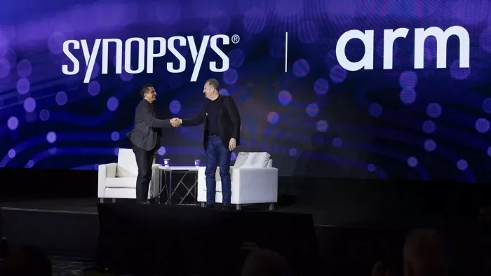
Arm and Synopsys: Delivering an Integrated, Nine-Stage “Silicon-to-System” Chip Design Flow
After more than three decades, the relationship between Arm and Synopsys continues to redefine the semiconductor industry. And the fusion of our expertise and technology continues to reshape chip design flows.
With AI workloads growing, the demand for energy-efficient hardware mounting, and design cycles shrinking, this enduring partnership is more important than ever.
By integrating Arm’s Compute Subsystems (CSS) and Neoverse platform with our comprehensive suite of IP — including Foundation, Interface, and Security IP — and optimizing our design and verification tools for those integrated solutions, we’re enabling customers to develop superior chips with greater velocity.
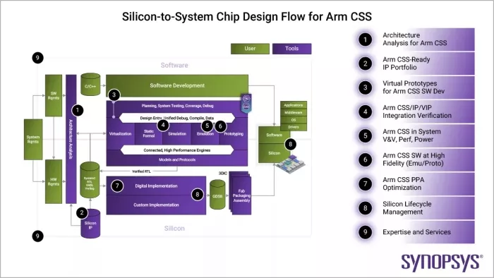
This includes a fully integrated, nine-stage “silicon-to-system” design flow that streamlines every step — from initial architecture analysis to silicon lifecycle management (SLM).
- Architecture analysis
Every successful chip design begins with a thorough architectural analysis. This involves estimating performance, power, and area (PPA) based on system requirements and anticipated workloads. Arm provides detailed domain models for its compute subsystems, while we offer tools for early-stage architecture optimization. Our solutions enable engineers to simulate how different configurations will behave, identify bottlenecks, and estimate resource usage. For example, network-on-chip (NoC) analysis helps teams determine the best way to partition chiplets and optimize interconnects for AI tasks. - IP integration
Integrating third-party IP — such as memory controllers, interfaces, and security blocks — is essential for building robust systems-on-chip (SoCs). Our portfolio includes IP blocks for PCI Express (PCIe), DDR, high-bandwidth memory (HBM), and other technologies, all optimized for Arm platforms. These IP blocks are designed to work seamlessly with Arm CSS, enabling out-of-the-box functionality and scalability for diverse applications. Standardized interfaces ensure compatibility and simplify integration, reducing design time and risk. - Virtual prototyping for software development
Developing software before physical hardware is available accelerates time-to-market and helps teams debug complex systems early. With our virtual prototyping solutions, software engineers can create pre-implementation representations of their designs to develop and test code in a virtual environment using Arm and Synopsys IP. Additionally, our virtual development kits enhance Arm’s fixed virtual platforms (FVPs), enabling firmware development for AI workloads. - Subsystem integration and verification
Once IP blocks are integrated, verifying the subsystem's functionality is crucial. We provide verification IP (VIP) and simulation tools to validate each component's interaction, ensuring proper communication and interoperability with Arm CSS. Our verification methods include block-level simulation, hardware emulation, and protocol testing using real or virtual traffic. Early detection of bugs and interface mismatches saves significant engineering effort and helps ensure the final silicon meets design goals. - Hardware-assisted verification (emulation and prototyping)
Simulation alone can’t capture all the complexities of real-world workloads. Hardware-assisted verification — using our emulation platforms such as ZeBu and HAPS — bridges the gap between simulation and silicon bring-up. These platforms allow engineers to run actual software on accurate hardware models, validating system-level behavior, performance, power consumption, and compliance with Arm SystemReady. Hardware-assisted verification is particularly effective for validating computing and AI accelerators under real-world AI workloads. - High-fidelity software development
When customer designs are ready for RTL-accurate hardware-assisted verification, software development transitions to hybrid environments that combine virtualization, hardware emulation, and FPGA-based prototyping — including Arm Fast Models and Arm RTL. Teams also use fully hardware-based setups for at-speed interface bring-up. Running operating systems, drivers, and AI applications on near-final hardware representations helps uncover hidden issues and optimize performance. And techniques like hybrid emulation with real devices facilitate rapid driver initialization and compliance testing, providing insights that are impossible to obtain through simulation alone. - Digital implementation and PPA optimization
Once the design is verified, engineers focus on digital implementation — translating the logical design into physical silicon. Our design tools offer flows tailored for specific Arm architectures. These flows optimize PPA by balancing speed, power consumption, and silicon area. Our QuickStart Integration Kits (QIKs) for Arm-based designs streamline the process, helping teams achieve aggressive performance targets and efficient layouts. - Silicon lifecycle management (SLM)
The silicon journey doesn’t end at tapeout — ongoing management is essential for reliability and performance. We work closely with Arm to ensure the System Monitoring Control Framework (SMCF) effectively manages a wide range of on-chip sensors and monitors, including our SLM IP solutions that track temperature, process variations, and operational metrics throughout the silicon lifecycle. These insights help manufacturers optimize production, identify field issues, and extend the life of deployed systems. SLM is increasingly important as chips become more complex and are deployed in mission-critical AI and cloud environments. - Expertise and services
Beyond tools and IP, our partnership with Arm offers deep expertise — spanning architectural modeling, system setup, implementation, and optimization. We support customers through every stage, helping teams implement best practices and overcome design challenges. This holistic approach reduces risk, accelerates development, and delivers high-quality silicon tailored for specific markets and workloads.
Customer impact: real-world proof points
The effectiveness of our integrated solutions with Arm is evident in customer outcomes across the industry:
- Microsoft leveraged Synopsys architecture analysis tools in conjunction with Arm system models to optimize Arm CMN NoC interconnects, catch design issues early, and accurately estimate power consumption. This early insight contributed to more reliable, efficient chip architectures.
- Rebellions, an AI startup, used Synopsys virtual prototyping and hybrid emulation tools that include Arm Fast Models to develop firmware and optimize AI workloads before hardware was available. This approach enabled fast, risk-reduced architectural experimentation, rapid software validation, and even pre-RTL LLM operation for their AI accelerator.
- As an example for protocol validation, Samsung utilized subsystem integration, verification, and ZeBu emulation to develop a high-performance CXL interface for storage applications. Hardware-assisted verification enabled faster debugging and greater design flexibility.
- Google dramatically accelerated driver initialization for PCIe by using hybrid emulation with real devices, achieving a 96x speed-up over traditional simulation and enabling faster, more efficient software development.
- Arm improved subsystem reliability and lifecycle management in their Morello design by implementing our SLM IP for on-chip monitoring and analytics.
Enabling the next wave of AI innovation
With integrated, holistic approaches becoming vital for modern SoC development, our collaboration with Arm and the nine-stage “silicon-to-system” design flow we’re delivering stand apart. By combining Arm’s advanced compute subsystems with our comprehensive IP, tools, and services, engineering teams can efficiently navigate the complexities of next-gen chip design.
Our partnership not only accelerates time-to-market but also delivers robust, scalable solutions for data centers, edge devices, and beyond — unlocking new possibilities for the era of pervasive intelligence.
Related Semiconductor IP
- Verification IP for C-PHY
- Band-Gap Voltage Reference with dual 2µA Current Source - X-FAB XT018
- 250nA-88μA Current Reference - X-FAB XT018-0.18μm BCD-on-SOI CMOS
- UCIe D2D Adapter & PHY Integrated IP
- Low Dropout (LDO) Regulator
Related Blogs
- Using AI to Accelerate Chip Design: Dynamic, Adaptive Flows
- Meet Synopsys.ai Copilot, Industry's First GenAI Capability for Chip Design
- Calligo Enables Next-Gen Computing at Scale with Synopsys Digital Design Flow
- Synopsys Collaborates with Arm to Drive Automotive Design Excellence