Advancing In-Memory Computing: A Global Effort to Build More Efficient AI Hardware

Artificial intelligence is driving one of the most significant architectural shifts the semiconductor industry has seen in decades. As AI workloads continue to expand away from the cloud to increasingly capable edge devices, traditional computing architectures are struggling to keep pace. One of the biggest edge-AI challenges is to keep power consumption as low as possible, as a growing share of energy in modern AI systems is consumed not by computation itself, but by moving data between processors and memory This growing inefficiency is often described as the “memory wall,” where data movement, rather than computation, dominates system energy consumption.
 Reducing this data movement has become one of the central challenges in next-generation AI hardware design. This is why researchers around the world are exploring in-memory computing (IMC), an architectural approach that performs certain computations directly within memory arrays instead of repeatedly transferring data between memory and compute units.
Universities, research institutes, and semiconductor companies are increasingly investing in collaborative programs aimed at advancing these technologies. One recent example is a Republic of Korea national initiative focused on energy-efficient AI semiconductors, where Weebit ReRAM serves as a foundational memory element.

Above: A quick search on Google Scholar shows the increase in research publications over the past several years for “In-Memory Computing,” showing a clear trend as AI workloads have increased. (Note: this doesn’t include publications using other synonymous terms such as “Compute in Memory,” Processing in Memory,” etc.)
Why IMC Is Attracting Global Attention
Many AI workloads rely on repeated vector-matrix multiplication operations. These are the mathematical core of neural networks. In conventional computing architectures, the data required for these operations constantly moves between memory and processing units. This repeated data movement creates both performance limitations and significant energy overhead.
IMC addresses this challenge by enabling computation to take place directly within the memory array. When neural network weights are stored within memory cells that can also support computation, matrix operations can be performed directly where the data resides.
In crossbar arrays, the physical behavior of current flowing through resistive devices naturally performs the multiply-accumulate operations required for neural networks. By applying voltages across rows and measuring currents along columns, the array leverages Ohm’s and Kirchhoff’s laws to compute vector-matrix multiplications in parallel.
This can lead to substantial improvements in energy efficiency, processing throughput, latency, and overall system scalability. For AI workloads, particularly those running at the edge, these improvements could be transformative.

Above: From conventional (Von Neumann) computing architectures to IMC
Why Continued Research is Essential
While the concept of IMC has been studied for many years, translating it into practical semiconductor products requires advances across multiple layers of technology. Unlike conventional digital processors, IMC systems involve complex interactions between memory device physics, circuit design and signal conversion, system architecture and machine-learning algorithms.
For example, device-level characteristics such as variability, noise, and retention behavior can directly influence the accuracy of AI inference. Peripheral circuitry such as analog-to-digital converters (ADCs) and digital-to-analog converters (DACs) must also be optimized to support efficient and accurate system operation.
Because these effects are tightly coupled, simulation alone cannot fully capture system behavior. Real progress requires experimentation with silicon implementations that integrate memory devices, circuits, and algorithms in realistic environments.
This need for cross-disciplinary collaboration is one of the reasons national research initiatives have become increasingly important in advancing IMC technologies.
A Collaborative Research Effort in Korea
The Republic of Korea is funding a national research program focused on developing energy-efficient compute-in-memory technologies for future AI hardware.
The initiative brings together semiconductor companies, academic institutions, and research organizations to explore how emerging memory technologies can enable new computing architectures optimized for artificial intelligence.
Participants include the Daegu Gyeongbuk Institute of Science and Technology, Seoul National University, Chungbuk National University, and the Electronics and Telecommunications Research Institute (ETRI).
Weebit is contributing our ReRAM technology, while DB HiTek, a leading Korean foundry, provides the manufacturing platform used to fabricate silicon devices for the program. In addition, AnalogAI plans to commercialize products based on the resulting ACiM blocks.
A key objective of the program is to develop and validate a compute-in-memory chip built around large ReRAM device arrays integrated with commercial CMOS circuitry. The project targets arrays of 256×256 cells or larger, capable of storing multiple resistance levels to represent neural-network weights. These arrays will be combined with optimized peripheral circuitry to demonstrate energy efficiency approaching 200 TOPS/W.
In parallel, the consortium will develop integration flows that combine ReRAM devices with standard CMOS processes that can be used in commercial foundries, enabling realistic silicon implementations. The work also includes modeling, design tools, and algorithm-level techniques to address challenges such as device variation, noise, retention behavior, and conversion inefficiencies. Validating these approaches in silicon is an important step toward practical IMC systems.
By combining device innovation with commercial semiconductor manufacturing processes, the initiative aims to move IMC technologies beyond early research demonstrations and toward practical system implementations.
Why ReRAM Is Well Suited for In-Memory Computing
Emerging non-volatile memory (NVM) technologies are widely viewed as key enablers of IMC architectures. Among them, Resistive RAM (ReRAM) has attracted significant interest due to its combination of scalability, efficiency, and compatibility with standard semiconductor processes.
ReRAM stores data as programmable resistance states within a simple two-terminal memory cell. When arranged in crossbar arrays, these devices can naturally support the parallel operations required for neural-network computations (MAC operations).
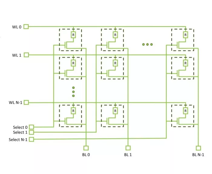
Above: The simple structure and scalability of ReRAM makes it ideal for IMC
ReRAM also offers several advantages that support IMC development:
- Multi-level programmable states for representing neural-network weights
- Highly parallel crossbar architectures for efficient matrix operations
- Low switching energy to enable energy-efficient computation
- Compatibility with standard CMOS manufacturing processes
Together, these characteristics allow ReRAM arrays to act as both memory storage and computational fabric, helping reduce the energy cost of data movement in AI systems.
Explore ReRAM NVM IP:
Building the Future of AI Hardware
AI is rapidly reshaping the semiconductor landscape, driving innovation across memory technologies, processor architectures, and system design. Advancing IMC will require sustained research, silicon validation, and collaboration across the global semiconductor ecosystem.
Programs like the Korean national IMC initiative illustrate how industry, academia, and government can work together to explore new computing paradigms capable of meeting the growing demands of AI. With emerging memory technologies such as ReRAM providing new architectural possibilities, these efforts are helping lay the groundwork for the next generation of energy-efficient AI hardware.
To read more about Weebit ReRAM in AI, read, “Pushing the Boundaries of Memory,” and visit our new AI Inference applications page.
Related Semiconductor IP
Related Blogs
- The Silent Guardian of AI Compute - PUFrt Unifies Hardware Security and Memory Repair to Build the Trust Foundation for AI Factories
- RISC-V: An Open Standard - Backed by a Global Community - to Enable Open Computing for All
- Small Language Models: Efficient Arm Computing Enables a Custom AI Future
- What It Will Take to Build a Resilient Automotive Compute Ecosystem
Latest Blogs
- Advancing In-Memory Computing: A Global Effort to Build More Efficient AI Hardware
- Satellite communications are no longer as secure as assumed
- Why Hardware Monitoring Needs Infrastructure, Not Just Sensors
- Why Post-Quantum Cryptography Doesn’t Replace Classical Cryptography
- The Silent Guardian of AI Compute - PUFrt Unifies Hardware Security and Memory Repair to Build the Trust Foundation for AI Factories